Design Files
1 design file
-
Printed Circuit Boards and Schematics
OrCAD Design Files for the MPC8544 and MPC8533
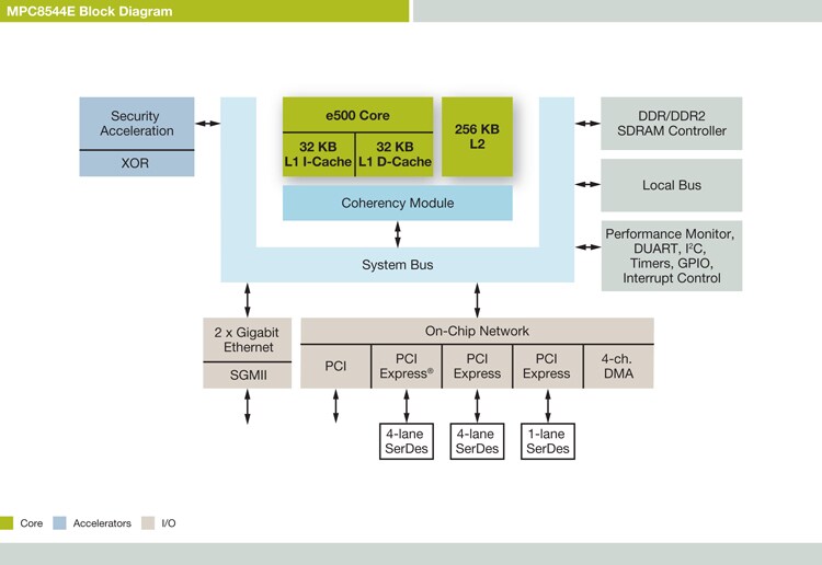
The MPC8544E PowerQUICC® III is designed to offer the unique combination of high performance, exceptional integration and lower overall power consumption required for networking, communications and industrial control applications.
The MPC8544E includes a high-performance e500 processor core built on Power Architecture® technology, enhanced peripherals and high-speed interconnect technology to balance processor performance with I/O system throughput enabling clock speeds scaling from 667 MHz up to 1.067 GHz. Third-generation PowerQUICC III processors are based on NXP®.s 90 nanometer (nm) silicon-on-insulator (SOI) copper interconnect process technology, which is designed to enable the processors to deliver higher performance with lower power dissipation.
The MPC8544E processor offers a wide range of high-speed connectivity options, including Gigabit Ethernet (GbE) interfaces with SGMII support and multiple PCI Express® connections. Support for these high-speed interfaces should enable scalable connectivity to network processors and/or ASICs in the data plane while the PowerQUICC III is designed to handle complex, computationally demanding control plane processing tasks. The MPC8544E is also designed to provide support for legacy PowerQUICC III interfaces such as PCI, I²C, dual universal asynchronous receiver/transmitters (DUART) and local bus connections. These processors are also designed to feature a next-generation double data rate (DDR2) memory controller, enhanced GbE support, v2 e500 double precision floating point and the field proven 90 nm PowerQUICC III integrated security engines.
Key Advantages
Access to the errata document for this device requires an NDA. Contact your local NXP Sales Office or NXP Authorized Distributor.
Part numbers include: MPC8544CVJALFA, MPC8544CVJANGA, MPC8544CVJAQGA, MPC8544ECVJALFA, MPC8544ECVJANGA, MPC8544ECVJAQGA, MPC8544EVJALFA, MPC8544EVJANGA, MPC8544EVJAQGA, MPC8544EVJARJA, MPC8544EVTANGA, MPC8544EVTAQGA, MPC8544EVTARJA, MPC8544VJALFA, MPC8544VJANGA, MPC8544VJAQGA, MPC8544VJARJA, MPC8544VTALFA, MPC8544VTAQGA, MPC8544VTARJA.
Quick reference to our documentation types.
1-5 of 39 documents
1 design file
2 hardware offerings
3 software files
Note: For better experience, software downloads are recommended on desktop.
To get further assistance directly from NXP, please see our Engineering Services.
1-5 of 14 engineering services


To find a complete list of our partners that support this product, please see our Partner Marketplace.
1-5 of 6 trainings