
BGA7210
700 MHz to 3800 MHz high linearity variable gain amplifier
The BGA7210 MMIC is an extremely linear Variable Gain Amplifier (VGA), operating from 0.7 GHz to 3.8 GHz. The maximum gain is 30 dB. It has an attenuation range of 31.5 dB. At its minimum attenuation setting it has a maximum output power of 21 dBm, an IP3O of 39 dBm and a noise figure of 6.5 dB.
The current consumption can be optimized per attenuation setting allowing for optimized overall system performance. The current consumption and attenuation level are controlled through a Serial Peripheral Interface (SPI). The current can be reduced to 120 mA. Optimal linearity performance is obtained at 185 mA. The BGA7210 has a fast switching power-down pin to further reduce current consumption during idle time.
The BGA7210 has been designed and qualified for the severe mission profile of cellular base stations, but its outstanding RF performance and interfacing flexibility make it suitable for a wide variety of applications.
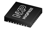
The BGA7210 is housed in a 32 pins 5 mm x 5 mm leadless HVQFN32 package.
| Symbol | Parameter | Conditions | Min | Typ/Nom | Max | Unit |
|---|---|---|---|---|---|---|
| Static characteristics | ||||||
| VCC | supply voltage | 4.75 | 5 | 5.25 | V | |
| ICC(tot) | total supply current | VCC = 5 V; maximum current | 160 | 195 | 230 | mA |
| Dynamic characteristics: f = 700 Mhz to 3760 MHz; Tamb = 25 °C; output is per frequency band matched to 50 Ω; unless otherwise specified. | ||||||
| Gp | power gain | 2200 MHz ≤ f ≤ 2800 MHz; VCC = 5 V; minimum attenuation | 25 | 28 | 31 | dB |
| NF | noise figure | 3400 MHz ≤ f ≤ 3800 MHz; maximum attenuation | 28.5 | 32 | dB | |
| NF | noise figure | 2200 MHz ≤ f ≤ 2800 MHz; minimum attenuation | 7 | 9 | dB | |
| IP3O | output third-order intercept point | 700 MHz ≤ f ≤ 1400 MHz; Δf = 10 MHz; minimum attenuation | 34 | 39 | dBm | |
| IP3O | output third-order intercept point | 1400 MHz ≤ f ≤ 1700 MHz; Δf = 10 MHz; maximum attenuation | 33 | dBm | ||
| PL(1dB) | output power at 1 dB gain compression | IDD = 185 mA; VDD = 5 V; 700 MHz ≤ f ≤ 2800 MHz; minimum attenuation | 18 | 21 | dBm | |
| frange | frequency range | 700 | 3800 | MHz | ||
| Grange | gain range | 30.5 | dB | |||
| Pin | Symbol | Description | Simplified outline | Graphic symbol |
|---|---|---|---|---|
| 1 | GND | ground | No image available. | ![]() |
| 2 | GND | ground | ||
| 3 | GND | ground | ||
| 4 | GND | ground | ||
| 5 | GND | ground | ||
| 6 | GND | ground | ||
| 7 | GND | ground | ||
| 8 | GND | ground | ||
| 9 | GND | ground | ||
| 10 | GND | ground | ||
| 11 | n.c. | not connected | ||
| 12 | RF_OUT | RF otput | ||
| 13 | GND | ground | ||
| 14 | GND | ground | ||
| 15 | VCC2 | Supply voltage to amplifier 2 (5 V) | ||
| 16 | VDDA | Analog supply voltage to DSA (5 V) | ||
| 17 | VCC1 | Supply voltage to amplifier 1 (5 V) | ||
| 18 | GND | ground | ||
| 19 | VDDD | Digital supply voltage to digital controller (5 V) | ||
| 20 | SER_OUT | SPI data output (3.3 V) | ||
| 21 | SS | SPI slave select (0 = select; 1 = deselect) | ||
| 22 | SER_IN | SPI data input | ||
| 23 | CLK | SPI clock input | ||
| 24 | PUPMXG/PWRDN | Power-up gain attenuation / power down | ||
| 25 | GND | ground | ||
| 26 | GND | ground | ||
| 27 | GND | ground | ||
| 28 | GND | ground | ||
| 29 | RF_IN | RF input | ||
| 30 | n.c. | not connected | ||
| 31 | GND | ground | ||
| 32 | GND | ground |
| Package Version | Package Name | Package Description | Reference Codes | Issue Date |
|---|---|---|---|---|
| SOT617-3 | HVQFN32 | plastic thermal enhanced very thin quad flat package; no leads; 32 terminals; body 5 x 5 x 0.85 mm | MO-220 (JEDEC); | 2002-10-22 |
| Type number | Orderable part number | Chemical content | RoHS | Leadfree conversion date | RHF | IFR (FIT) | MTBF (hours) | MSL | MSL LF |
|---|---|---|---|---|---|---|---|---|---|
| BGA7210 | BGA7210X | BGA7210 | week 42, 2012 | 1 | 1 | ||||
| BGA7210 | BGA7210,515 | BGA7210 | Always Pb-free | 2 | 2 |
| File name | Title | Type | Format | Date |
|---|---|---|---|---|
| BGA7210 | 700 MHz to 3800 MHz high linearity variable gain amplifier | Data sheet | 2013-01-29 | |
| AN11152 | Reducing the Spurs at RF_out caused by the biasing choke during fast switching on and off in TDD system | Application note | 2012-01-20 | |
| AN11251 | BGA7210 Operation Frequency Extension Down to 400 MHz | Application note | 2012-09-20 | |
| 75017347 | Enabling the Mobile Experience | Brochure | 2013-02-05 | |
| NXP_Digital_VGA_BGA7210__BGA7204_Leaflet_939775017239 | NXP Digital VGA BGA7210 & BGA7204 Leaflet | Leaflet | 2012-05-10 | |
| UM10480 | Variable gain amplifier BGA7210 | User manual | 2011-07-26 |
Sample orders normally take 2-4 days for delivery.
If you do not have a direct account with NXP our network of global and regional distributors is available and equipped to support you with NXP samples. As a NXP customer you also have the option to order samples via our sales organisation.
Variable gain amplifier BGA7210 customer evaluation kit
Do you want to ask technical questions to an NXP expert?
Please select one of the following options:
Follow us