Design Files
1 design file
-
Models
nx3l2g66 IBIS model
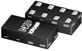
The NX3L2G66 is a dual low-ohmic single-pole single-throw analog switch. Each switch has two input/output terminals (nY and nZ) and an active HIGH enable input (nE). When pin nE is LOW, the analog switch is turned off.
Schmitt trigger action at the enable input (nE) makes the circuit tolerant to slower input rise and fall times. The NX3L2G66 allows signals with amplitude up to VCC to be transmitted from nY to nZ; or from nZ to nY. Its low ON resistance (0.5 Ω) and flatness (0.13 Ω) ensures minimal attenuation and distortion of transmitted signals.

Part numbers include: NX3L2G66GT.
Quick reference to our documentation types.
1-5 of 8 documents
Please wait while your secure files are loading.
1 design file
Please wait while your secure files are loading.