In my previous post ‘A look at die-level heat transfer’, I
introduced a ‘detailed’ MOSFET die model and demonstrated how it could be used to predict device
junction temperatures for short power pulses. The detailed thermal simulation model of a typical NXP D2PAK device is
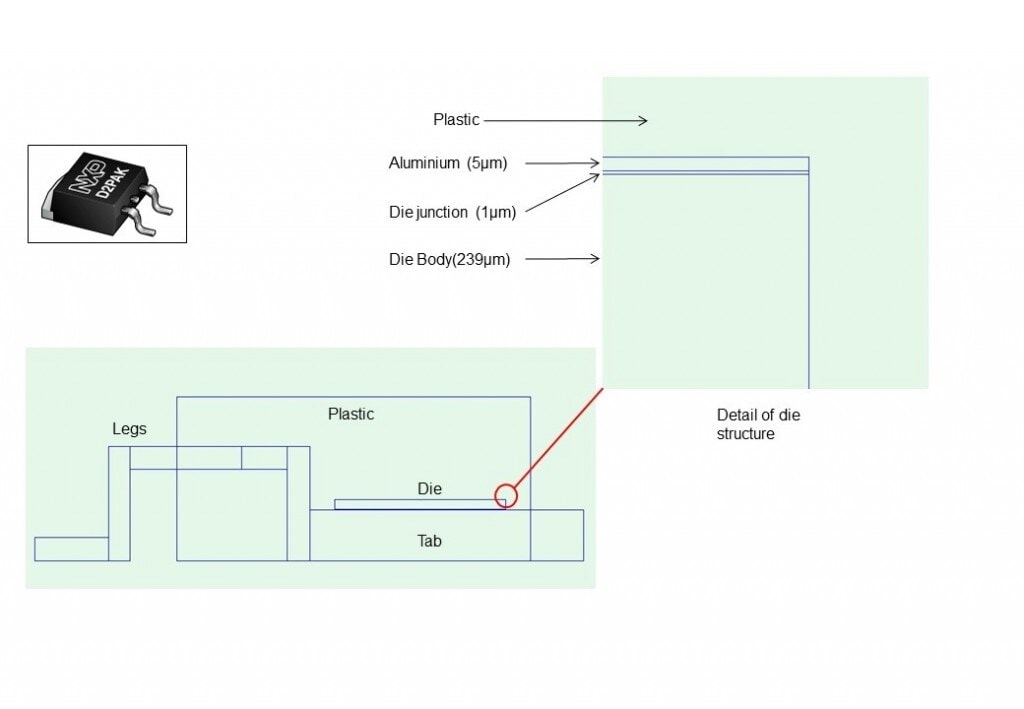
shown again in Figure 1. The full description of the model can be found in my previous post, but it is worth
repeating here that the dissipating part of the die model is the 1 µm ‘Die Junction’ layer. The
other parts of the model are capable of conducting heat energy, but have no heat dissipation of their own.

Figure 1 An NXP D2PAK MOSFET (top left), its detailed thermal model (bottom left) and
detail of the die structure (right).
Although predicting temperatures is a very important goal for thermal simulation, there are other results that may be
equally useful, which simulations can provide. In particular, simulations can help us understand the flow
of heat energy within a system over time and therefore develop a better appreciation of the relative importance of the
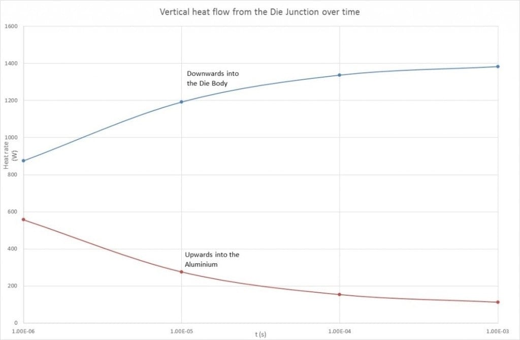
various elements within that thermal system. The graph of Figure 2 shows the vertical flow of heat energy out of the
Die Junction as a function of time.

Figure 2 The vertical flow of heat energy out of the Die Junction over time.
The graph of Figure 2 suggests that, even though the aluminum layer is itself quite thin (5 µm), a significant
amount of heat energy can flow into it during short time intervals. However the long-term benefit of the aluminum
is limited by the plastic material above it, which has an extremely low thermal conductivity. So as the thermal
energy from the die ‘charges up’ the thermal capacitance of the aluminum, the thermal gradient
between the die and aluminum becomes less and so the flow of heat into the aluminum also decreases.
At this point, we have a perfect opportunity to try out one of the ‘what if’ analyses I mentioned in my
post – Simulation and reality. Given that a thin layer of metal on the
top of the die is capable of absorbing significant heat energy in the short term, what would happen if we soldered a
copper clip to the top of the die? In effect creating a ‘Top-clip D2PAK’. This would be quite
difficult (though not impossible) to achieve in reality, but in simulation it is the work of mere minutes. First we
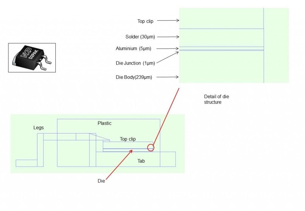
create the new model, with top clip and solder, as shown in Figure 3.

Figure 3 A detailed die model of D2PAK with top clip and solder.
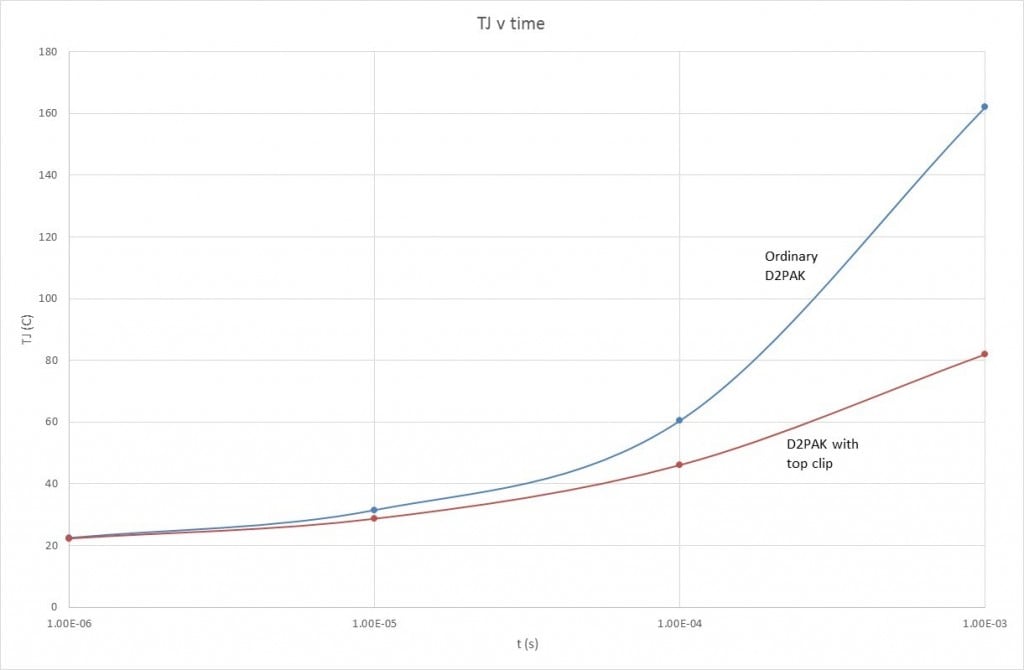
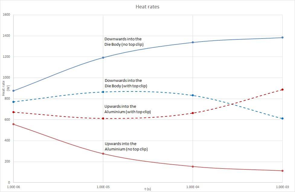
Now we can run the simulations again and compare the temperature results (Figure 4) and heat flow results (Figure 5).

Figure 4 Simulated temperature results for the D2PAK with and without top clip.

Figure 5 The vertical flow of heat energy out of the Die Junction over time for the D2PAK
with and without top clip.
Clearly the top clip has made a big difference! Figure 4 indicates a significant decrease in TJ at 100
µs and 1 ms when the top clip is present. Similarly Figure 5 demonstrates a large increase in the heat energy
flowing out of the top of the die and ultimately into the top clip. In effect, the simulation indicates that we are
able to influence the time-dependent thermal behavior of the die by adding an extra heat path to the top of the
die.
In my next post I will explore this theme further, taking a real device – the NXP LFPAK – as an example of how a top clip can be used to influence
the thermal response of a power MOSFET device.
PS. We really haven’t made any ‘top clip D2PAK’ MOSFETs, nor are we planning to in the future,
so I’m afraid samples are not available. Sorry!
