Low-Ohmic Single-Pole Single-Throw Analog Switch
NX3V1G66 アラートの受信
- アーカイブス
- このページには、製造中止(生産終了)となった製品の情報が記載されています。本ページに記載されている仕様および情報は、過去の参考情報です。
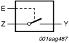
The NX3V1G66 provides one single–pole single–throw analog switch function. It has two input/output terminals (Y and Z) and an active HIGH enable input pin (E). When pin E is LOW, the analog switch is turned off.
Schmitt trigger action at the enable input (E) makes the circuit tolerant to slower input rise and fall times across the entire VCC range from 1.4 V to 4.3 V.
The NX3V1G66 allows signals with amplitude up to VCC to be transmitted from Y to Z or from Z to Y. Its ultra–low ON resistance (0.3 Ω) and flatness (0.1 Ω) ensures minimal attenuation and distortion of transmitted signals.
製品詳細
Features
System Features
- Wide supply voltage range from 1.4 V to 4.3 V
- Very low ON resistance (peak):
- 0.8 Ω (typical) at VCC = 1.4 V
- 0.5 Ω (typical) at VCC = 1.65 V
- 0.3 Ω (typical) at VCC = 2.3 V
- 0.25 Ω (typical) at VCC = 2.7 V
- 0.25 Ω (typical) at VCC = 4.3 V
- High noise immunity
- ESD protection:
- HBM JESD22– A114F Class 3A exceeds 7500 V
- MM JESD22– A115– A exceeds 200 V
- CDM AEC– Q100– 011 revision B exceeds 1000 V
- CMOS low– power consumption
- Latch– up performance exceeds 100 mA per JESD78B Class II Level A
- Direct interface with TTL levels at 3.0 V
- Control input accepts voltages above supply voltage
- High current handling capability (500 mA continuous current under 3.3 V supply)
- Specified from – 40 °C to +85 °C and from – 40 °C to +125 °C