ハードウェア
5 ハードウェア提供
-
 エミュレータ、プローブ、プログラマ
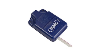
Universal Multilink開発インターフェース注目
-
エミュレータ、プローブ、プログラマ
LFBDMPGMRS08FW
-
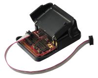
 エミュレータ、プローブ、プログラマ
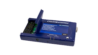
PEmicro Cyclone programmer
-
追加ハードウェアを利用可能 パートナー・ソリューションの特集を表示.
-
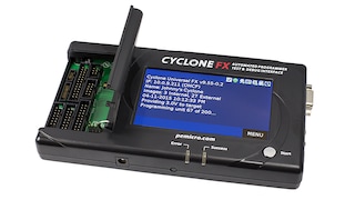
 エミュレータ、プローブ、プログラマ
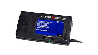
PEmicro Cyclone FX programmer
-
 エミュレータ、プローブ、プログラマ
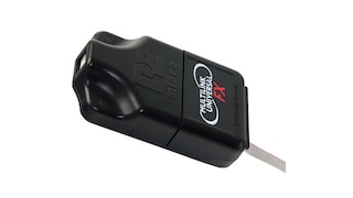
Universal Multilink FX高速開発インターフェース