デザイン・ファイル
2 設計・ファイル
-
プリント基板と回路図
Symbols for MPC85x0 - Mentor Graphics format
-
プリント基板と回路図
Symbols for MPC85x0 - EDIF format
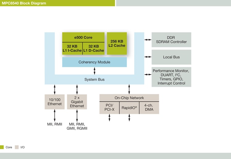
Addressing the needs for higher compute density and lower system cost, Our MPC8540 integrated host processor is designed to provide the highest level of performance and integration available today. The MPC8540 is Our first device utilizing the e500 core, is the industry's first RapidIO®-enabled processor, and provides dual gigabit ethernet controllers. Balancing processor performance with I/O system throughput, the MPC8540 is a powerful control element for network routers and switches, storage subsystems, network appliances, and print and imaging devices.
Contact your local NXP Sales Office or NXP Authorized Distributor.
部品番号: MPC8540CVT667JC, MPC8540VT667LC, MPC8540VT833LC.
クイック・リファレンス ドキュメンテーションの種類.
1-5 の 64 ドキュメント
2 設計・ファイル
4 ソフトウェア・ファイル
注: より快適にご利用いただくために、ソフトウェアのダウンロードはデスクトップで行うことを推奨します。