3.0 A, 1.0 MHz Integrated DDR Switch-Mode Power Supply
MC34712 アラートの受信
- 新規採用非推奨
- このページでは、新規設計を推奨しない製品に関する情報を掲載しています。
The NXP® MC34712 is a highly-integrated, space-efficient, low-cost, single-synchronous buck switching regulator with integrated N-channel power MOSFETs.
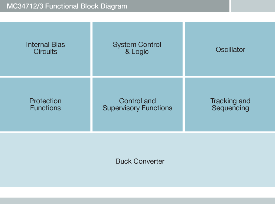
- High performance point-of-load (PoL) power supply with the ability to track an external reference voltage
- Its high efficient 3 A sink and source capability combined with its voltage tracking/sequencing ability and tight output regulation makes it ideal to provide the termination voltage for modern data buses such as DDR memory buse
- Provides a buffered output VREF to the memory chipset
- Offers flexibility of many control, supervisory, and protection functions to allow for easy implementation of complex designs
製品詳細
ブロック図
Features
System Features
- Integrated N-channel power MOSFETs
- Input voltage operating range from 3 V to 6 V
- Accurate output voltage, ranging from 0.7 V to 1.35 V
- Accurate buffered reference output voltage
- Programmable switching frequency range from 200 kHz to 1.0 MHz with a default of 1.0 MHz
- Over current limit and short circuit protection
- Thermal shutdown
- Output over-voltage and under-voltage detection
- Active low power good output signal
- Active low standby and shutdown inputs
- Single buck regulator
- Output current 3 A
- Output voltage 1.5 V
Product Longevity Program
- This product is included in NXP®.s product longevity program, with assured supply for a minimum of 10 years after launch
部品番号: MC34712EP.
設計・リソース

エンジニアリング・サービス
NXPから直接サポートを受けるには、以下のサイトをご覧ください。 エンジニアリング・サービス.
1 エンジニアリング・サービス
-
インディペンデントデザインハウス (IDH)
Embedded Software Design

本製品をサポートするパートナーの一覧は、 パートナーマーケットプレイス.