-
OM13319
-
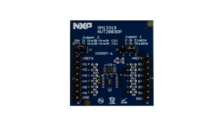
NVT2003DP Demo Board.
The NVT2003DP (OM13319), NVT2004TL (OM13316) and NVT2006PW (OM13323) demo boards are designed to evaluate the NXP® 3-channel, 4-channel and 6-channel bi-directional voltage level translators. The demo boards interface between device I/Os operating at different voltage levels. Since the NVT2003DP, NVT2004TL, and NVT2006PW devices are passive devices, pull-up resistors may be needed depending on the I/O interface type (totem pole or open-drain), a difference in translation voltage, and the translation direction (high to low-voltage, low to high-voltage, or bi-directional). The NVT2003DP, NVT2004TL and NVT2006PW devices allow translations between any voltages from 1.0 V to 5.5 V.
J1 (3 pins) to control NVT device enable (pin 2-3 on)
or disable (pin 1-2 on)
NVT2003DP Demo Board.
Quick reference to our documentation types.