

Design Files
2 design files
-
Models
GLT2008 IBIS model
-
Symbols and Footprints
GTL2008PW_TSSOP28-CAD Symbol and PCB Footprint – BXL File
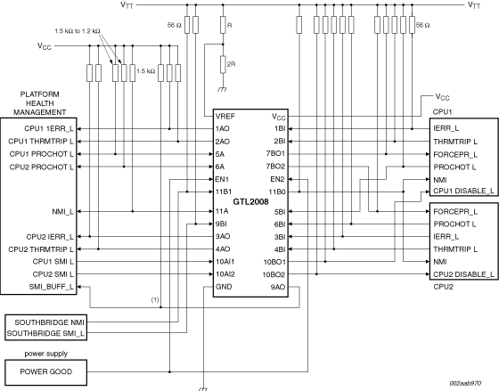
The GTL2008 is a customized translator between dual Xeon processors, Platform Health Management, South Bridge and Power Supply LVTTL and GTL signals.
Functionally and footprint identical to the GTL2007, the GTL2008 LVTTL and GTL outputs were changed to put them into a high-impedance state when EN1 and EN2 are LOW, with the exception of 11BO because its normal state is LOW, so it is forced LOW. EN1 and EN2 will remain LOW until VCC is at normal voltage, the other inputs are in valid states and VREF is at its proper voltage to assure that the outputs will remain high-impedance through power-up.
The GTL2008 has the enable function that disables the error output to the monitoring agent for platforms that monitor the individual error conditions from each processor. This enable function can be used so that false error conditions are not passed to the monitoring agent when the system is unexpectedly powered down. This unexpected power-down could be from a power supply overload, a CPU thermal trip, or some other event of which the monitoring agent is unaware.
A typical implementation would be to connect each enable line to the system power good signal or the individual enables to the VRD power good for each processor.
Typically Xeon processors specify a VTT of 1.1 V to 1.2 V, as well as a nominal Vref of 0.73 V to 0.76 V. To allow for future voltage level changes that may extend Vref to 0.63 of VTT(minimum of 0.693 V with VTT of 1.1 V) the GTL2008 allows a minimum Vref of 0.66 V. Characterization results show that there is little DC or AC performance variation between these Vref levels.
Part numbers include: GTL2008PW.
Quick reference to our documentation types.
5 documents
2 design files