Design Files
Receive the full breakdown. See the product footprint and more in the eCad file.
NXP® 56F836X and 56F816X digital signal controllers belong to the 56800E core-based DSC family. They combine digital signal processing and microcontroller functionalities on a single chip, with a flexible set of peripherals.
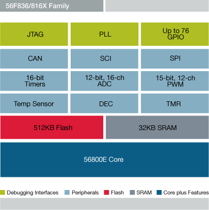
Note: To see the product features close this window.
Part numbers include: MC56F8165VFGE, MC56F8167VPYE, MC56F8365MFGE, MC56F8365VFGE, MC56F8366MFVE, MC56F8366VFVE, MC56F8367MPYE, MC56F8367VPYE, MC56F8367VVFE, S56F8365W0MFGE.
|
|
|
|
|
|
|
|---|---|---|---|---|---|
|
|
|
|
|
|
|
|
|
|
|
|
|
|
|
|
|
|
|
|
|
|
|
|
|
|
|
|
|
|
|
|
|
|
|
|
|
|
|
|
|
|
|
|
|
|
|
|
|
|
|
|
|
|
|
|
|
|
|
|
|
|
|
|
|
|
|
|
|
|
Quick reference to our documentation types.
1-5 of 70 documents
Please wait while your secure files are loading.
Receive the full breakdown. See the product footprint and more in the eCad file.

Receive the full breakdown. See the product footprint and more in the eCad file.
1-5 of 6 hardware offerings
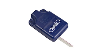
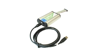
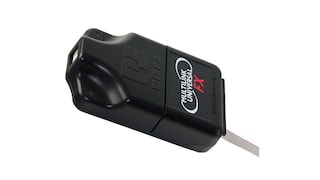
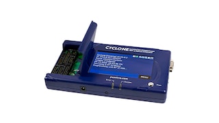
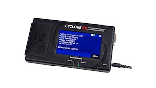
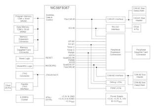
Quick reference to our software types.
1-5 of 21 software files
Additional software available. View our featured partner solutions.
Note: For better experience, software downloads are recommended on desktop.
Please wait while your secure files are loading.
1 software offerings

To find additional partner offerings that support this product, visit our Partner Marketplace.
1 engineering service

There are no results for this selection.
To find additional partner offerings that support this product, visit our Partner Marketplace.