Compact List
- No Longer Manufactured
- OM13529UL
PCAL6524 Fm+ I²C 24-bit GPIO Demo Board
- This page contains information on a product that is no longer manufactured (discontinued). Specifications and information herein are available for historical reference only.
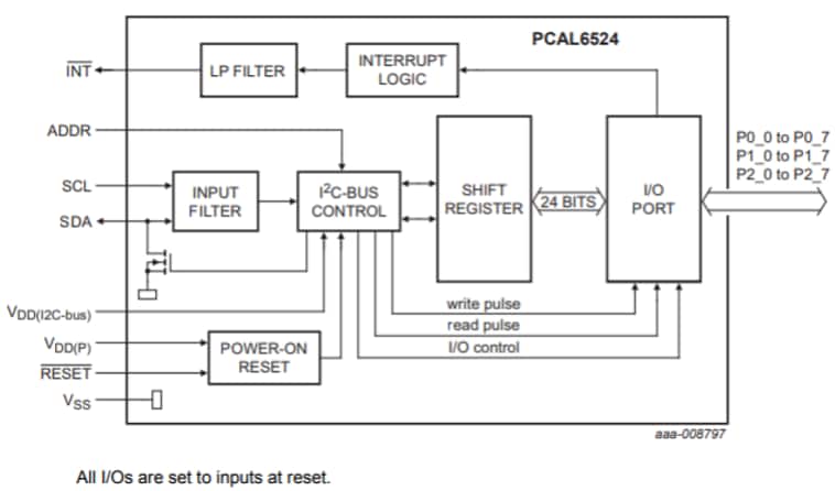
The OM13529 is the demo board for the PCAL6524. The PCAL6524 is a 24-bit general purpose I/O expander that provides remote I/O expansion for most NXP microcontroller families via the Fast-mode Plus (Fm+) I2C-bus interface. The ultra-low-voltage interface allows for direct connection to a microcontroller operating down to 0.8 V.
Product Details
Features
Connectivity
- 1 MHz Fast-mode Plus I2C-bus
- 5.5 V tolerant I/O ports and 3.6 V tolerant I2C-bus pins
Power Management
- An operating power supply voltage range of 0.8 V to 3.6 V on the I2C-bus side
- Allows bidirectional voltage-level translation and GPIO expansion between 0.8 V to 3.6 V SCL/SDA and 1.8 V, 2.5 V, 3.3 V, 5.5 V Port P
- Low standby current consumption: 2.0 µA typical at 3.3 V VDD(p)
- Internal power-on reset
-
ESD protection exceeds JESD 22
- 2000 V Human-Body Model (A114-A)
- 1000 V Charged-Device Model (C101)
Expansion Port
- I2C-bus to parallel port expander
Key Features
- Latch-up performance exceeds 100 mA per JESD 78, Class II
- Latched outputs with 25 mA drive maximum capability for directly driving LEDs
-
Schmitt trigger action allows slow input transition and better
switching noise immunity at the SCL and SDA inputs
- Vhys = 0.05 V (typical) at 0.8 V
- Vhys = 0.18 V (typical) at 1.8 V
- Vhys = 0.33 V (typical) at 3.3 V
- Packages offered: TSSOP32, HUQFN32, VFBGA36
- Noise filter on SCL/SDA inputs
- Active LOW reset input (RESET)
- Open-drain active LOW interrupt output (INT)