
Application Note (8)
Data Sheet (1)
Package Information (2)
Supporting Information (2)
-
Footprint for wave soldering[QFP-SQFP-TQFP-WAVE]
-
Footprint for wave soldering[PLCC-WAVE]
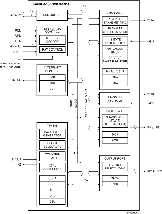
The SC28L92 is a pin and function replacement for the SCC2692 and SC26C92 operating at 3.3 V or 5 V supply with added features and deeper FIFOs. Its configuration on power-up is that of the SC26C92. Its differences from the SCC2692 and SC26C92 are: 16 character receiver, 16 character transmit FIFOs, watchdog timer for each receiver, mode register 0 is added, extended baud rate and overall faster speeds, programmable receiver and transmitter interrupts. (Neither the SC26C92 nor the SCC2692 is being discontinued.)
Pin programming will allow the device to operate with either the Motorola or Intel bus interface. The bit 3 of the MR0A register allows the device to operate in an 8 byte FIFO mode if strict compliance with the SC26C92 FIFO structure is required.
The NXP Semiconductors SC28L92 Dual Universal Asynchronous Receiver/Transmitter (DUART) is a single-chip CMOS-LSI communications device that provides two full-duplex asynchronous receiver/transmitter channels in a single package. It interfaces directly with microprocessors and may be used in a polled or interrupt driven system with modem and DMA interface.
The operating mode and data format of each channel can be programmed independently. Additionally, each receiver and transmitter can select its operating speed as one of 28 fixed baud rates; a 16x clock derived from a programmable counter/timer, or an external 1x or 16x clock. The baud rate generator and counter/timer can operate directly from a crystal or from external clock inputs. The ability to independently program the operating speed of the receiver and transmitter make the DUART particularly attractive for dual-speed channel applications such as clustered terminal systems.
Each receiver and transmitter is buffered by 8 or 16 character FIFOs to minimize the potential of receiver overrun, transmitter underrun and to reduce interrupt overhead in interrupt driven systems. In addition, a flow control capability is provided via RTS/CTS signaling to disable a remote transmitter when the receiver buffer is full.
Also provided on the SC28L92 are a multipurpose 7-bit input port and a multipurpose 8-bit output port. These can be used as general purpose I/O ports or can be assigned specific functions (such as clock inputs or status/interrupt outputs) under program control.
The SC28L92 is available in three package versions: PLCC44, QFP44, and HVQFN48.
Choose a diagram:
|
|
|
|
|
|
|
|---|---|---|---|---|---|
|
|
|
|
|
|
|
|
|
|
|
|
|
|
|
|
|
|
|
|
|
|
|
|
|
|
|
|
|
|
|
|
|
|
|
|
|
|
|
|
|
|
|
|
|
|
|
|
|
|
|
|
|
|
|
|
|
|
|
|
|
|
|
|
|
|
|
|
|
|
Quick reference to our documentation types
1-10 of 13 documents
Compact List
2 design files
Receive the full breakdown. See the product footprint and more in the eCad file.