Technical content and expertise to help jump start your design and get you to production faster.
Start your designDownload our latest development and embedded software solutions.
Expedite time-to-market with our extensive lineup of development kits.
Jump-start your design with proven hardware and software solutions.
Get the latest specifications in our technical documentation library.
Further your technical expertise with online and in-person instruction.
Get comprehensive paid support to fast-track your product development.
Design ideas, demo videos, quality answers. Connect with NXP professionals and other knowledgeable designers ready to help.
Software, documentation, evaluation tools. The resources to build comprehensive solutions and accelerate your time to market.
Access our design resource libraryWe're always looking for passionate and talented people to work with us.
Join our teamArchived content is no longer updated and is made available for historical reference only.
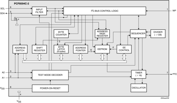
The PCF8594C-2 is a floating gate Electrically Erasable Programmable Read Only Memory (EEPROM) with 4 kbits (512 x 8-bit) non-volatile storage. By using an internal redundant storage code, it is fault tolerant to single bit errors. This feature dramatically increases the reliability compared to conventional EEPROMs. Power consumption is low due to the full CMOS technology used. The programming voltage is generated on-chip, using a voltage multiplier.
Data bytes are received and transmitted via the serial I²C-bus. Up to four PCF8594C-2 devices may be connected to the I²C-bus. Chip select is accomplished by two address inputs (A1 and A2).
Timing of the E/W cycle is carried out internally, thus no external components are required. Programming Time Control (PTC), Pin 7, must be connected to either VDD or left open-circuit. There is an option of using an external clock for timing the length of an E/W cycle.
Evaluation and Development Boards