Compact List
- No Longer Manufactured
- DSP56011
Symphony® Digital Audio DSP
- This page contains information on a product that is not recommended for new designs.
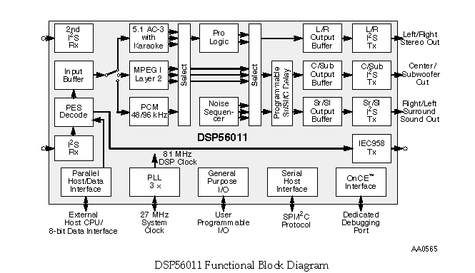
The DSP56011 is a high-performance programmable Digital Signal Processor (DSP) specifically developed for Digital Versatile Disk (DVD), High-Definition Television (HDTV), and Advanced Set-top audio decoding. The DSP56011 is optimized with audio-specific peripherals and customized memory configuration, and uses Motorola's certified software for Dolby AC-3; 5.1 Channel Surround, Dolby Pro Logic, and MPEG®1 Layer 2.
The block diagram shows the functional blocks of the DSP56011. In addition, the DSP56011 offers switchable memory space configuration, a large user-definable Program ROM and two independent data RAMs and ROMs, a Serial Audio Interface (SAI), Serial Host Interface (SHI), parallel Host Interface (HI) with Direct Memory Access (DMA) (DMA) for communicating with other processors, dedicated I/O lines, on-chip Phase Lock Loop (PLL), On-Chip Emulation (OnCE) port, and on-chip Digital Audio Transmitter (DAX).