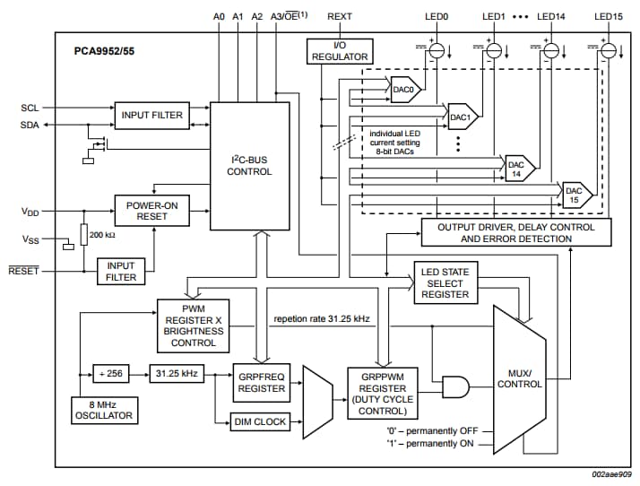
The PCA9952 and PCA9955 are I²C-bus controlled 16-channel constant current LED
driver optimized for dimming and blinking 57 mA Red/Green/Blue/Amber (RGBA) LEDs in
amusement products. Each LEDn output has its own 8-bit resolution (256 steps) fixed
frequency individual PWM controller that operates at 31.25 kHz with a duty cycle that is
adjustable from 0 % to 99.6 % to allow the LED to be set to a specific brightness value. An
additional 8-bit resolution (256 steps) group PWM controller has both a fixed frequency of
122 Hz and an adjustable frequency between 15 Hz to once every 16.8 seconds with a
duty cycle that is adjustable from 0 % to 99.6 % that is used to either dim or blink all LEDs
with the same value.
Each LEDn output can be off, on (no PWM control), set at its individual PWM controller
value or at both individual and group PWM controller values. The PCA9952 and PCA9955
operate with a supply voltage range of 3 V to 5.5 V and the constant current sink LEDn
outputs allow up to 40 V for the LED supply. The output peak current is adjustable with an
8-bit linear DAC from 225 µA to 57 mA.
These devices have built-in open, short load and overtemperature detection circuitry. The
error information from the corresponding register can be read via the I²C-bus. Additionally,
a thermal shutdown feature protects the device when an internal junction temperature
exceeds the limit allowed for the process.
The PCA9952 and PCA9955 devices have Fast-mode Plus (Fm+) I²C-bus interface. Fm+
devices offer higher frequency (up to 1 MHz) or more densely populated bus operation
(up to 4000 pF).
The PCA9952 is identical to PCA9955 except for the following differences:
- The PCA9952 has only three hardware address pins compared to four on PCA9955
- The PCA9952 has an output enable pin (OE) and the PCA9955 does not
The active LOW output enables input pin (OE), available only on PCA9952, blinks all the
LEDs outputs and can be used to externally PWM the outputs, which is useful when
multiple devices need to be dimmed or blinked together without using software control.
Software programmable LED Group and three Sub Call I²C-bus addresses allow all or
defined groups of PCA9952/55 devices to respond to a common I²C-bus address,
allowing, for example, all red LEDs to be turned on or off at the same time or marquee
chasing effect, thus minimizing I²C-bus commands. On power-up, PCA9952/55 will have
a unique Sub Call address to identify it as a 16-channel LED driver. This allows mixing of
devices with different channel widths. Four hardware address pins on PCA9955 allow up
to 16 devices on the same bus. In the case of PCA9952, three hardware address pins
allow up to 8 devices on the same bus.
The Software Reset (SWRST) function allows the controller to perform a reset of the
PCA9952/55 through the I²C-bus, identical to the Power-On Reset (POR) that initializes
the registers to their default state causing the output current switches to be OFF (LED off).
This allows an easy and quick way to reconfigure all device registers to the same
condition.