Data Sheet (1)
-
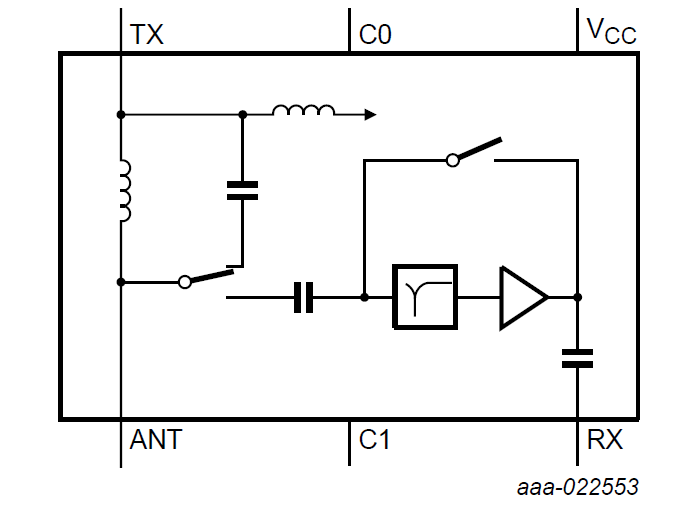
Archived - WLAN LNA + Switch[BGS8458]
The BGS8458, also known as the WLAN3101C, is a fully integrated MMIC Low-Noise Amplifier and SP2T switch for transmit path. For WLAN applications in the 4.9 GHz to 5.925 GHz ISM band. Manufactured using high performance QUBiC eighth generation SiGe:C technology of NXP®.
The BGS8458 couples good noise figure, linearity, efficiency, low insertion loss CMOS switches with the process-stability, and -ruggedness, that are the hallmarks of SiGe:C technology.
The BGS8458 has a 1.2 mm × 1.4 mm footprint HX2SON6 package and a maximum thickness of 330 μm.
|
|
|
|
|
|
|
|---|---|---|---|---|---|
|
|
|
|
|
|
|
|
|
|
|
|
|
|
|
|
|
|
|
|
|
|
|
|
|
|
|
|
|
|
|
|
|
|
|
|
|
|
|
|
|
|
|
|
|
|
|
|
|
|
|
|
|
|
|
|
|
|
|
|
|
|
|
|
|
|
|
|
|
|
Receive the full breakdown. See the product footprint and more in the eCad file.
