S32G Network Board Setup Guides
Contents of this document
-
Out of the Box
-
Get Software
-
Plug It In
-
Build, Run
Sign in to save your progress. Don't have an account? Create one.
Purchase your S32G Vehicle Network Processing Evaluation Board 3
1. Out of the Box
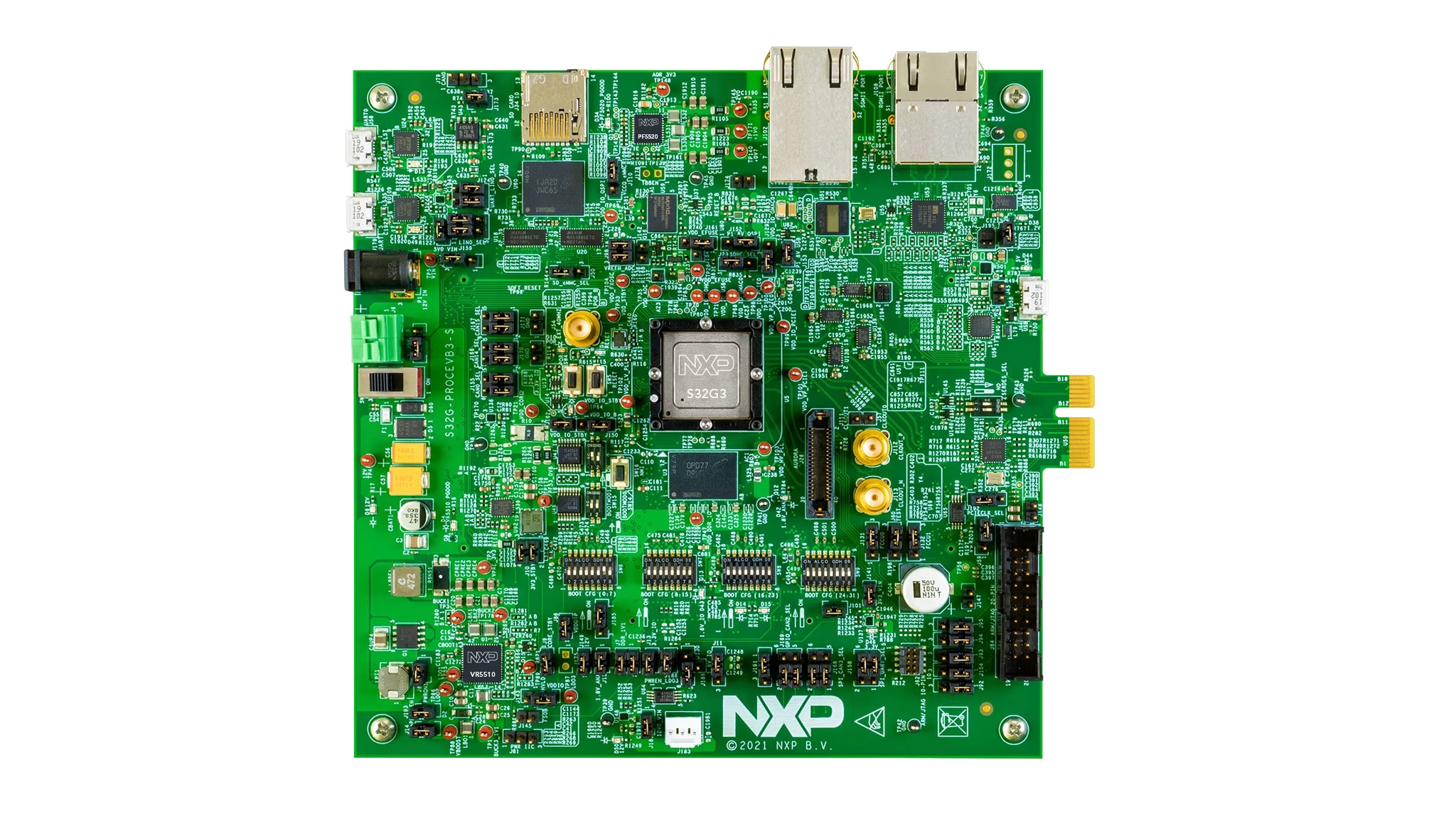
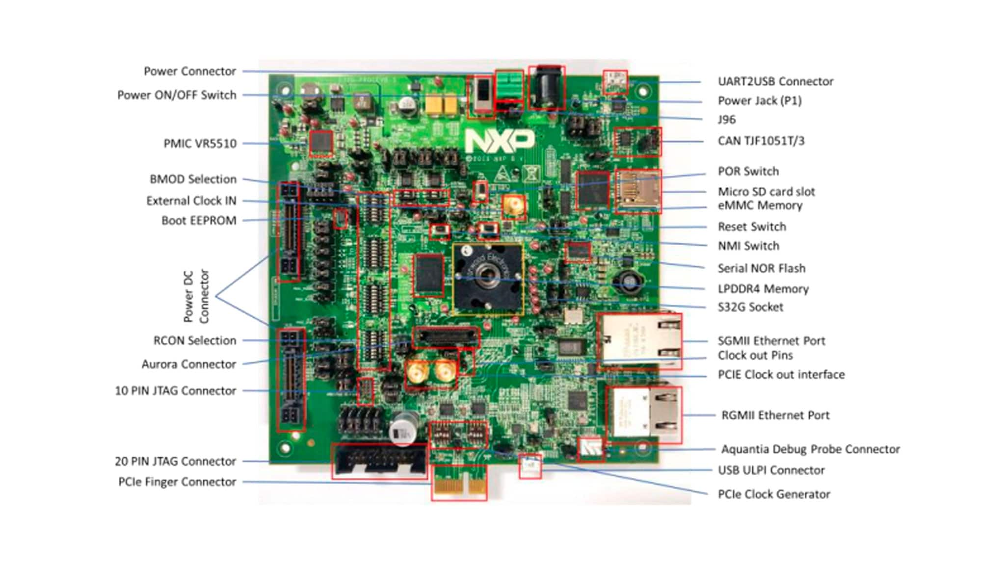
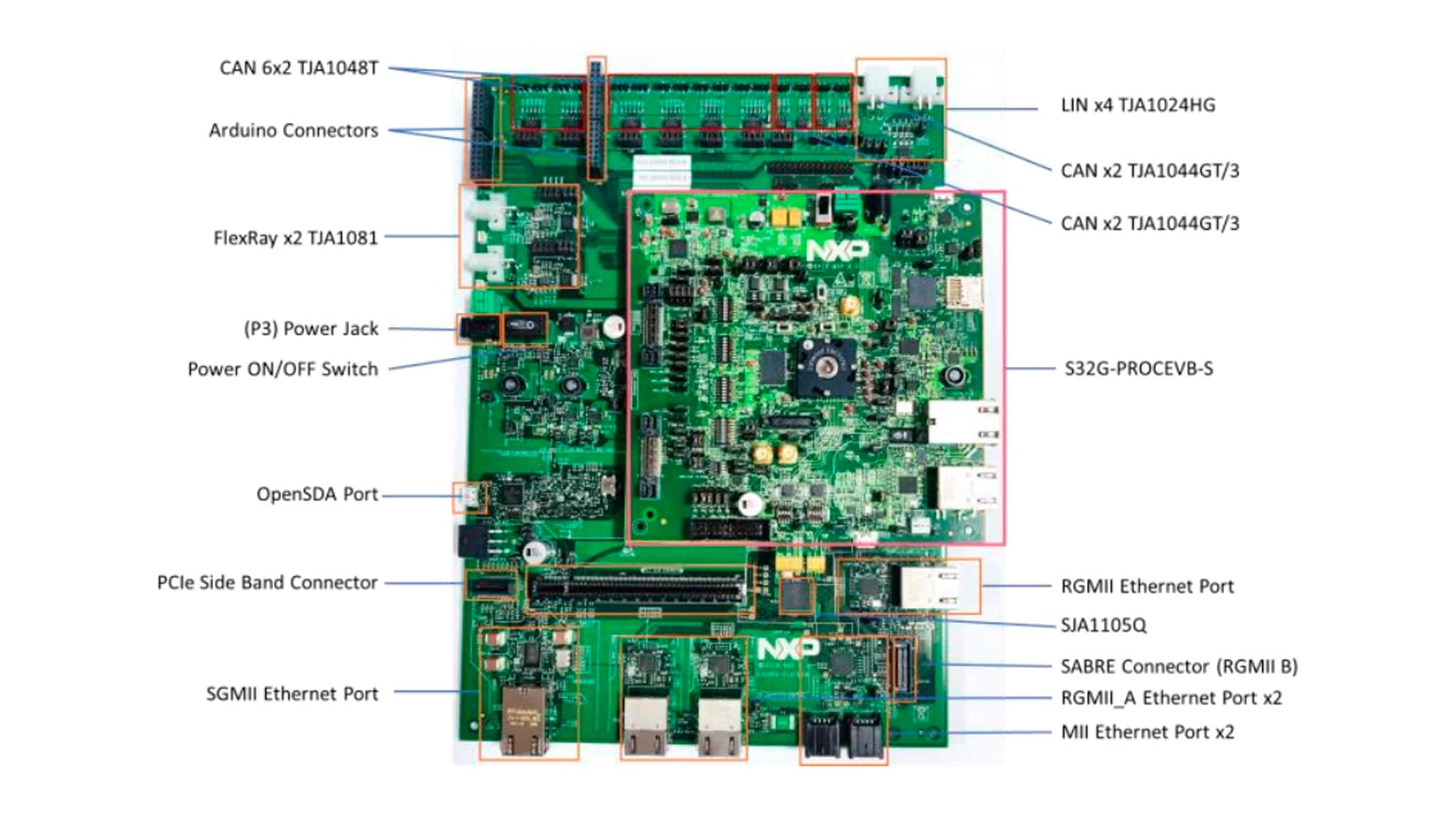
1.1 Get to Know the Evaluation Board
1.2 Get to Know the Processor Module
2. Get Software
Learn how to use the Automotive Software Package Manager
2.1 Install Tera Term for Console
Tera Term is open source free software terminal emulator supporting UTF-8 protocol. Now TTSSH supports SSH2 protocol (original version supports SSH1).
Tera Term is now Tera Term Pro 2.3, the succession version. It is officially recognized by the original author.
2.2 Install FTDI CDM WHQL Driver
FTDI CDM v2.12.28 WHQL driver for serial configuration from FTDI chip.
2.3 Install Win32 Disk Imager
A Windows tool for writing images to USB sticks or SD/CF cards.
2.4 Install Packet Sender Application
A free utility to send and receive network packets: TCP, UDP and SSL.
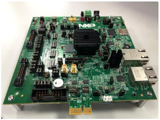
3. Plug It In
Let’s take it for a test drive.
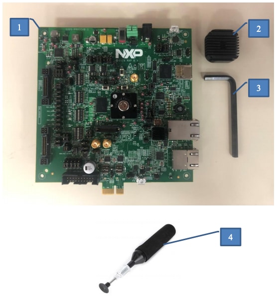
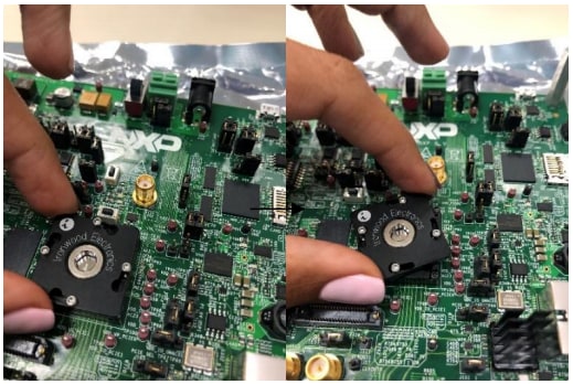
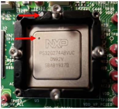
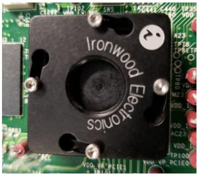
3.1 Install S32G Socket and Heatsink
| 1 | S32G-PROCEVB-S: S32G Processor Module with Ironwood Electronics SG-BGA-6124 Socket |
| 2 | M4159 Heatsink |
| 3 | Hex key |
| 4 | Timiy Vacuum Pen Tool |
Watch the video to install the socket and heatsink. You can also use the step-by-step guide.
- Turn the socket screw to the left to loosen the top of the socket
- Remove the socket cover by turning it to the left and lifting up. Set it aside
- Use the vacuum tool to pick up and remove the compression plate from the socket. Set it aside
- Using the vacuum tool, pick up the S32G device and place it in the socket base.
- Remove the screw completely from the socket cover with the hex key
- Using the vacuum tool, install the compression plate on top of the S32G device
- Replace the socket cover and turn to the right to lock in place
- Rotate the heatsink slowly clockwise until initial contact with the compression plate. Turn it 1/4 turn to make good contact. Do not over-stress the socket
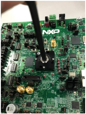
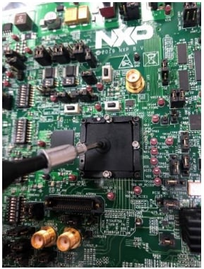

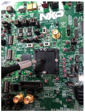
Do not force the heatsink.
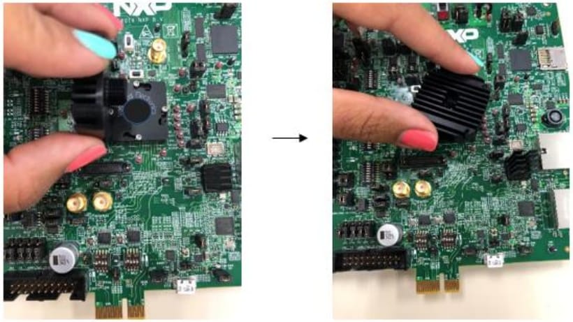
When the installation is complete, it should look like the picture:
3.2 Plug in the 12 V Power Supply
When the S32G-PROCEVB-S is stacked on the S32GRV-PLATEVB:
Jumper J96 on the S32G-PROCEVB-S should be in position 1-2, Only the S32GRVPLATEVB needs to be powered.
Connect power supply to the 12 V power jack P3 on S32GRV-PLATEVB.
When the S32G-PROCEVB-S is used standalone:
Jumper J96 should be in position 2-3.
Connect power supply to the 12 V power jack P1 on S32G-PROCEVB-S.
4. Build, Run
4.1 Setup Tera Term 4 Console
- Open Tera Term on Windows PC
- Select the serial port to which the micro USB
J58of the S32G-PROCEVB-S is connected and click OK - Go to Setup → Serial Port and select
115200as the baud rate
4.2 Power On the S32G-VNP-EVB3
Switch on the power switch SW1 on the S32GRV-PLATEVB and power switch SW10 on the S32G-PROCEVB-S.
4.3 Run Diagnostics
The Diagnostics Utility is auto-executed from the SD card.
The console display on Tera Term shows the status of the diagnostic tests.
RTD Examples
Kickstart your RTD journey with these handy examples. We've rounded up some of the most common use cases to get you inspired and moving forward.
Users can copy the path directly into their window once the RTD is downloaded.
RTD Examples for S32G2
ADC
C:\NXP\S32DS.3.6.1\S32DS\software\PlatformSDK_S32XX_4_0_0\RTD\Adc_TS_T40D11M40I2R0\examples\S32DS\S32G2\Adc_example_S32G274A_M7ADC SAR CTU IP
C:\NXP\S32DS.3.6.1\S32DS\software\PlatformSDK_S32XX_4_0_0\RTD\Adc_TS_T40D11M40I2R0\examples\S32DS\S32G2\Adc_Sar_Ctu_Ip_example_S32G274A_M7CAN
C:\NXP\S32DS.3.6.1\S32DS\software\PlatformSDK_S32XX_4_0_0\RTD\Can_TS_T40D11M40I2R0\examples\S32DS\S32G2\Can_example_S32G274A_M7FLEXCAN IP
C:\NXP\S32DS.3.6.1\S32DS\software\PlatformSDK_S32XX_4_0_0\RTD\Can_TS_T40D11M40I2R0\examples\S32DS\S32G2\FlexCAN_Ip_Example_S32G274A_M7CRC
C:\NXP\S32DS.3.6.1\S32DS\software\PlatformSDK_S32XX_4_0_0\RTD\Crc_TS_T40D11M40I2R0\examples\S32DS\S32G2\Crc_Example_S32G274A_M7CRC IP
C:\NXP\S32DS.3.6.1\S32DS\software\PlatformSDK_S32XX_4_0_0\RTD\Crc_TS_T40D11M40I2R0\examples\S32DS\S32G2\Crc_Ip_Example_S32G274A_M7CRYPTO CMAC CTR
C:\NXP\S32DS.3.6.1\S32DS\software\PlatformSDK_S32XX_4_0_0\RTD\Crypto_TS_T40D11M40I2R0\examples\S32DS\S32G2\Crypto_CmacCtr_S32G274A_M7CRYPTO SYMMETRIC PRIMITIVES
C:\NXP\S32DS.3.6.1\S32DS\software\PlatformSDK_S32XX_4_0_0\RTD\Crypto_TS_T40D11M40I2R0\examples\S32DS\S32G2\Crypto_SymmetricPrimitives_S32G274A_M7HSE IP
C:\NXP\S32DS.3.6.1\S32DS\software\PlatformSDK_S32XX_4_0_0\RTD\Crypto_TS_T40D11M40I2R0\examples\S32DS\S32G2\Hse_Ip_AesEncAsyncIrq_S32G274A_M7DIO
C:\NXP\S32DS.3.6.1\S32DS\software\PlatformSDK_S32XX_4_0_0\RTD\Dio_TS_T40D11M40I2R0\examples\S32DS\S32G2\Dio_Example_S32G274A_M7SIUL2 DIO IP
C:\NXP\S32DS.3.6.1\S32DS\software\PlatformSDK_S32XX_4_0_0\RTD\Dio_TS_T40D11M40I2R0\examples\S32DS\S32G2\Siul2_Dio_Ip_Example_S32G274A_M7EEP
C:\NXP\S32DS.3.6.1\S32DS\software\PlatformSDK_S32XX_4_0_0\RTD\Eep_TS_T40D11M40I2R0\examples\S32DS\S32G2\Eep_example_S32G274A_M7USDHC IP
C:\NXP\S32DS.3.6.1\S32DS\software\PlatformSDK_S32XX_4_0_0\RTD\Eep_TS_T40D11M40I2R0\examples\S32DS\S32G2\Usdhc_Ip_example_S32G274A_M7TH
C:\NXP\S32DS.3.6.1\S32DS\software\PlatformSDK_S32XX_4_0_0\RTD\Eth_TS_T40D11M40I2R0\examples\S32DS\S32G2\Eth_InternalLoopback_S32G274A_M7GMAC IP
C:\NXP\S32DS.3.6.1\S32DS\software\PlatformSDK_S32XX_4_0_0\RTD\Eth_TS_T40D11M40I2R0\examples\S32DS\S32G2\Gmac_Ip_InternalLoopback_S32G274A_M7FEE
C:\NXP\S32DS.3.6.1\S32DS\software\PlatformSDK_S32XX_4_0_0\RTD\Fee_TS_T40D11M40I2R0\examples\S32DS\S32G2\Fee_Example_S32G274A_M7FLS
C:\NXP\S32DS.3.6.1\S32DS\software\PlatformSDK_S32XX_4_0_0\RTD\Fls_TS_T40D11M40I2R0\examples\S32DS\S32G2\Fls_Example_S32G274A_M7QSPI IP
C:\NXP\S32DS.3.6.1\S32DS\software\PlatformSDK_S32XX_4_0_0\RTD\Fls_TS_T40D11M40I2R0\examples\S32DS\S32G2\Qspi_Ip_Example_S32G274A_M7FLEXRAY IP NODE 1
C:\NXP\S32DS.3.6.1\S32DS\software\PlatformSDK_S32XX_4_0_0\RTD\Fr_TS_T40D11M40I2R0\examples\S32DS\S32G2\Flexray_Ip_ExternalCommunication_node1_S32G274A_M7FLEXRAY IP NODE 2
C:\NXP\S32DS.3.6.1\S32DS\software\PlatformSDK_S32XX_4_0_0\RTD\Fr_TS_T40D11M40I2R0\examples\S32DS\S32G2\Flexray_Ip_ExternalCommunication_node2_S32G274A_M7FR NODE 1
C:\NXP\S32DS.3.6.1\S32DS\software\PlatformSDK_S32XX_4_0_0\RTD\Fr_TS_T40D11M40I2R0\examples\S32DS\S32G2\FR_ExternalCommunication_node1_S32G274A_M7FR NODE 2
C:\NXP\S32DS.3.6.1\S32DS\software\PlatformSDK_S32XX_4_0_0\RTD\Fr_TS_T40D11M40I2R0\examples\S32DS\S32G2\FR_ExternalCommunication_node2_S32G274A_M7GPT
C:\NXP\S32DS.3.6.1\S32DS\software\PlatformSDK_S32XX_4_0_0\RTD\Gpt_TS_T40D11M40I2R0\examples\S32DS\S32G2\Gpt_Example_S32G274A_M7PIT GPT IP
C:\NXP\S32DS.3.6.1\S32DS\software\PlatformSDK_S32XX_4_0_0\RTD\Gpt_TS_T40D11M40I2R0\examples\S32DS\S32G2\Pit_Gpt_Ip_Example_S32G274A_M7I²C IP
C:\NXP\S32DS.3.6.1\S32DS\software\PlatformSDK_S32XX_4_0_0\RTD\I2c_TS_T40D11M40I2R0\examples\S32DS\S32G2\I2c_Example_Ip_S32G274A_M7I²C
C:\NXP\S32DS.3.6.1\S32DS\software\PlatformSDK_S32XX_4_0_0\RTD\I2c_TS_T40D11M40I2R0\examples\S32DS\S32G2\I2c_Example_S32G274A_M7FTC ICU IP
C:\NXP\S32DS.3.6.1\S32DS\software\PlatformSDK_S32XX_4_0_0\RTD\Icu_TS_T40D11M40I2R0\examples\S32DS\S32G2\Ftm_Icu_Ip_CheckNofi_S32G274A_M7ICU
C:\NXP\S32DS.3.6.1\S32DS\software\PlatformSDK_S32XX_4_0_0\RTD\Icu_TS_T40D11M40I2R0\examples\S32DS\S32G2\Icu_CheckNofi_S32G274A_M7LIN
C:\NXP\S32DS.3.6.1\S32DS\software\PlatformSDK_S32XX_4_0_0\RTD\Lin_TS_T40D11M40I2R0\examples\S32DS\S32G2\Lin_Example_S32G274A_M7LIN IP
C:\NXP\S32DS.3.6.1\S32DS\software\PlatformSDK_S32XX_4_0_0\RTD\Lin_TS_T40D11M40I2R0\examples\S32DS\S32G2\Linflexd_Lin_Ip_Example_S32G274A_M7DMA IP
C:\NXP\S32DS.3.6.1\S32DS\software\PlatformSDK_S32XX_4_0_0\RTD\Mcl_TS_T40D11M40I2R0\examples\S32DS\S32G2\Dma_Ip_DmaTransfer_S32G274A_M7MCL
C:\NXP\S32DS.3.6.1\S32DS\software\PlatformSDK_S32XX_4_0_0\RTD\Mcl_TS_T40D11M40I2R0\examples\S32DS\S32G2\Mcl_DmaTransfer_S32G274A_M7CLOCK IP
C:\NXP\S32DS.3.6.1\S32DS\software\PlatformSDK_S32XX_4_0_0\RTD\Mcu_TS_T40D11M40I2R0\examples\S32DS\S32G2\Clock_Ip_Example_S32G274A_M7MCU
C:\NXP\S32DS.3.6.1\S32DS\software\PlatformSDK_S32XX_4_0_0\RTD\Mcu_TS_T40D11M40I2R0\examples\S32DS\S32G2\Mcu_Example_S32G274A_M7POWER IP
C:\NXP\S32DS.3.6.1\S32DS\software\PlatformSDK_S32XX_4_0_0\RTD\Mcu_TS_T40D11M40I2R0\examples\S32DS\S32G2\Power_Ip_Example_S32G274A_M7OCOTP
C:\NXP\S32DS.3.6.1\S32DS\software\PlatformSDK_S32XX_4_0_0\RTD\Ocotp_TS_T40D11M40I2R0\examples\S32DS\S32G2\Ocotp_Example_S32G274A_M7OCOTP IP
C:\NXP\S32DS.3.6.1\S32DS\software\PlatformSDK_S32XX_4_0_0\RTD\Ocotp_TS_T40D11M40I2R0\examples\S32DS\S32G2\Ocotp_Ip_Example_S32G274A_M7FTM OCU IP
C:\NXP\S32DS.3.6.1\S32DS\software\PlatformSDK_S32XX_4_0_0\RTD\Ocu_TS_T40D11M40I2R0\examples\S32DS\S32G2\Ftm_Ocu_Ip_Example_S32G274A_M7OCU
C:\NXP\S32DS.3.6.1\S32DS\software\PlatformSDK_S32XX_4_0_0\RTD\Ocu_TS_T40D11M40I2R0\examples\S32DS\S32G2\Ocu_Example_S32G274A_M7PLATFORM MULTICORE SINGLE ELF
C:\NXP\S32DS.3.6.1\S32DS\software\PlatformSDK_S32XX_4_0_0\RTD\Platform_TS_T40D11M40I2R0\examples\S32DS\S32G2\Platform_Multicore_SingleElf_Example_S32G2XXPMIC AUTOSAR
C:\NXP\S32DS.3.6.1\S32DS\software\PlatformSDK_S32XX_4_0_0\RTD\Pmic_TS_T40D11M40I2R0\examples\S32DS\S32G2\Pmic_Configuration_Autosar_Example_S32G274A_M7PMIC NON AUTOSAR
C:\NXP\S32DS.3.6.1\S32DS\software\PlatformSDK_S32XX_4_0_0\RTD\Pmic_TS_T40D11M40I2R0\examples\S32DS\S32G2\Pmic_Configuration_Non_Autosar_Example_S32G274A_M7PORT
C:\NXP\S32DS.3.6.1\S32DS\software\PlatformSDK_S32XX_4_0_0\RTD\Port_TS_T40D11M40I2R0\examples\S32DS\S32G2\Port_Example_S32G274A_M7SIUL2 PORT IP
C:\NXP\S32DS.3.6.1\S32DS\software\PlatformSDK_S32XX_4_0_0\RTD\Port_TS_T40D11M40I2R0\examples\S32DS\S32G2\Siul2_Port_Ip_Example_S32G274A_M7FTM PWM IP
C:\NXP\S32DS.3.6.1\S32DS\software\PlatformSDK_S32XX_4_0_0\RTD\Pwm_TS_T40D11M40I2R0\examples\S32DS\S32G2\Ftm_Pwm_Ip_Example_S32G274A_M7PWM
C:\NXP\S32DS.3.6.1\S32DS\software\PlatformSDK_S32XX_4_0_0\RTD\Pwm_TS_T40D11M40I2R0\examples\S32DS\S32G2\Pwm_Example_S32G274A_M7FTM QDEC IP
C:\NXP\S32DS.3.6.1\S32DS\software\PlatformSDK_S32XX_4_0_0\RTD\Qdec_TS_T40D11M40I2R0\examples\S32DS\S32G2\Ftm_Qdec_Ip_Example_S32G274A_M7QDEC
C:\NXP\S32DS.3.6.1\S32DS\software\PlatformSDK_S32XX_4_0_0\RTD\Qdec_TS_T40D11M40I2R0\examples\S32DS\S32G2\Qdec_Example_S32G274A_M7MPU
C:\NXP\S32DS.3.6.1\S32DS\software\PlatformSDK_S32XX_4_0_0\RTD\Rm_TS_T40D11M40I2R0\examples\S32DS\S32G2\Mpu_M7_Ip_Example_S32G274A_M7MSCM IP
C:\NXP\S32DS.3.6.1\S32DS\software\PlatformSDK_S32XX_4_0_0\RTD\Rm_TS_T40D11M40I2R0\examples\S32DS\S32G2\Mscm_Ip_Example_S32G274A_M7RM
C:\NXP\S32DS.3.6.1\S32DS\software\PlatformSDK_S32XX_4_0_0\RTD\Rm_TS_T40D11M40I2R0\examples\S32DS\S32G2\Rm_Example_S32G274A_M7RM MPU
C:\NXP\S32DS.3.6.1\S32DS\software\PlatformSDK_S32XX_4_0_0\RTD\Rm_TS_T40D11M40I2R0\examples\S32DS\S32G2\Rm_Mpu_M7_Example_S32G274A_M7RM MSCM
C:\NXP\S32DS.3.6.1\S32DS\software\PlatformSDK_S32XX_4_0_0\RTD\Rm_TS_T40D11M40I2R0\examples\S32DS\S32G2\Rm_Mscm_Example_S32G274A_M7RM SEMAPHORE
C:\NXP\S32DS.3.6.1\S32DS\software\PlatformSDK_S32XX_4_0_0\RTD\Rm_TS_T40D11M40I2R0\examples\S32DS\S32G2\Rm_Semaphore_Example_S32G274A_M7SEMAPHORE IP
C:\NXP\S32DS.3.6.1\S32DS\software\PlatformSDK_S32XX_4_0_0\RTD\Rm_TS_T40D11M40I2R0\examples\S32DS\S32G2\Semaphore_Ip_Example_S32G274A_M7XRDC IP
C:\NXP\S32DS.3.6.1\S32DS\software\PlatformSDK_S32XX_4_0_0\RTD\Rm_TS_T40D11M40I2R0\examples\S32DS\S32G2\Xrdc_Ip_Example_S32G274A_M7LPSPI IP
C:\NXP\S32DS.3.6.1\S32DS\software\PlatformSDK_S32XX_4_0_0\RTD\Spi_TS_T40D11M40I2R0\examples\S32DS\S32G2\Lpspi_Ip_Transfer_S32G274A_M7LPSPI
C:\NXP\S32DS.3.6.1\S32DS\software\PlatformSDK_S32XX_4_0_0\RTD\Spi_TS_T40D11M40I2R0\examples\S32DS\S32G2\Lpspi_Transfer_S32G274A_M7SPI IP
C:\NXP\S32DS.3.6.1\S32DS\software\PlatformSDK_S32XX_4_0_0\RTD\Spi_TS_T40D11M40I2R0\examples\S32DS\S32G2\Spi_Ip_Transfer_S32G274A_M7SPI
C:\NXP\S32DS.3.6.1\S32DS\software\PlatformSDK_S32XX_4_0_0\RTD\Spi_TS_T40D11M40I2R0\examples\S32DS\S32G2\Spi_Transfer_S32G274A_M7THERMAL
C:\NXP\S32DS.3.6.1\S32DS\software\PlatformSDK_S32XX_4_0_0\RTD\Thermal_TS_T40D11M40I2R0\examples\S32DS\S32G2\Thermal_example_S32G274A_M7TMU
C:\NXP\S32DS.3.6.1\S32DS\software\PlatformSDK_S32XX_4_0_0\RTD\Thermal_TS_T40D11M40I2R0\examples\S32DS\S32G2\TMU_example_S32G274A_M7UART IP
C:\NXP\S32DS.3.6.1\S32DS\software\PlatformSDK_S32XX_4_0_0\RTD\Uart_TS_T40D11M40I2R0\examples\S32DS\S32G2\Linflexd_Uart_Ip_Example_S32G274A_M7UART IP
C:\NXP\S32DS.3.6.1\S32DS\software\PlatformSDK_S32XX_4_0_0\RTD\Uart_TS_T40D11M40I2R0\examples\S32DS\S32G2\Uart_Example_S32G274A_M7WDOG HLD
C:\NXP\S32DS.3.6.1\S32DS\software\PlatformSDK_S32XX_4_0_0\RTD\Wdg_43_VR5510_TS_T40D11M40I2R0\examples\S32DS\S32G2\Wdg_VR5510_HLD_Example_S32G274A_M7WDOG IP
C:\NXP\S32DS.3.6.1\S32DS\software\PlatformSDK_S32XX_4_0_0\RTD\Wdg_43_VR5510_TS_T40D11M40I2R0\examples\S32DS\S32G2\Wdg_VR5510_IP_Example_S32G274A_M7SWT IP
C:\NXP\S32DS.3.6.1\S32DS\software\PlatformSDK_S32XX_4_0_0\RTD\Wdg_TS_T40D11M40I2R0\examples\S32DS\S32G2\Swt_Ip_Example_S32G274A_M7WDOG
C:\NXP\S32DS.3.6.1\S32DS\software\PlatformSDK_S32XX_4_0_0\RTD\Wdg_TS_T40D11M40I2R0\examples\S32DS\S32G2\Wdg_Example_S32G274A_M7RTD Examples for S32G3
ADC
C:\NXP\S32DS.3.6.1\S32DS\software\PlatformSDK_S32XX_4_0_0\RTD\Adc_TS_T40D11M40I2R0\examples\S32DS\S32G3\Adc_example_S32G399A_M7ADC SAR CTU IP
C:\NXP\S32DS.3.6.1\S32DS\software\PlatformSDK_S32XX_4_0_0\RTD\Adc_TS_T40D11M40I2R0\examples\S32DS\S32G3\Adc_Sar_Ctu_Ip_example_S32G399A_M7CAN
C:\NXP\S32DS.3.6.1\S32DS\software\PlatformSDK_S32XX_4_0_0\RTD\Can_TS_T40D11M40I2R0\examples\S32DS\S32G3\Can_example_S32G399A_M7FLEXCAN IP
C:\NXP\S32DS.3.6.1\S32DS\software\PlatformSDK_S32XX_4_0_0\RTD\Can_TS_T40D11M40I2R0\examples\S32DS\S32G3\FlexCAN_Ip_Example_S32G399A_M7CRC
C:\NXP\S32DS.3.6.1\S32DS\software\PlatformSDK_S32XX_4_0_0\RTD\Crc_TS_T40D11M40I2R0\examples\S32DS\S32G3\Crc_Example_S32G399A_M7CRC IP
C:\NXP\S32DS.3.6.1\S32DS\software\PlatformSDK_S32XX_4_0_0\RTD\Crc_TS_T40D11M40I2R0\examples\S32DS\S32G3\Crc_Ip_Example_S32G399A_M7CRYPTO CMAC CTR
C:\NXP\S32DS.3.6.1\S32DS\software\PlatformSDK_S32XX_4_0_0\RTD\Crypto_TS_T40D11M40I2R0\examples\S32DS\S32G3\Crypto_CmacCtr_S32G399A_M7CRYPTO SYMMETRIC PRIMITIVES
C:\NXP\S32DS.3.6.1\S32DS\software\PlatformSDK_S32XX_4_0_0\RTD\Crypto_TS_T40D11M40I2R0\examples\S32DS\S32G3\Crypto_SymmetricPrimitives_S32G399A_M7HSE IP
C:\NXP\S32DS.3.6.1\S32DS\software\PlatformSDK_S32XX_4_0_0\RTD\Crypto_TS_T40D11M40I2R0\examples\S32DS\S32G3\Hse_Ip_AesEncAsyncIrq_S32G399A_M7DIO
C:\NXP\S32DS.3.6.1\S32DS\software\PlatformSDK_S32XX_4_0_0\RTD\Dio_TS_T40D11M40I2R0\examples\S32DS\S32G3\Dio_Example_S32G399A_M7SIUL2 DIO IP
C:\NXP\S32DS.3.6.1\S32DS\software\PlatformSDK_S32XX_4_0_0\RTD\Dio_TS_T40D11M40I2R0\examples\S32DS\S32G3\Siul2_Dio_Ip_Example_S32G399A_M7EEP
C:\NXP\S32DS.3.6.1\S32DS\software\PlatformSDK_S32XX_4_0_0\RTD\Eep_TS_T40D11M40I2R0\examples\S32DS\S32G3\Eep_example_S32G399A_M7USDHC IP
C:\NXP\S32DS.3.6.1\S32DS\software\PlatformSDK_S32XX_4_0_0\RTD\Eep_TS_T40D11M40I2R0\examples\S32DS\S32G3\Usdhc_Ip_example_S32G399A_M7ETH
C:\NXP\S32DS.3.6.1\S32DS\software\PlatformSDK_S32XX_4_0_0\RTD\Eth_TS_T40D11M40I2R0\examples\S32DS\S32G3\Eth_InternalLoopback_S32G399A_M7GMAC IP
C:\NXP\S32DS.3.6.1\S32DS\software\PlatformSDK_S32XX_4_0_0\RTD\Eth_TS_T40D11M40I2R0\examples\S32DS\S32G3\Gmac_Ip_InternalLoopback_S32G399A_M7FEE
C:\NXP\S32DS.3.6.1\S32DS\software\PlatformSDK_S32XX_4_0_0\RTD\Fee_TS_T40D11M40I2R0\examples\S32DS\S32G3\Fee_Example_S32G399A_M7FLS
C:\NXP\S32DS.3.6.1\S32DS\software\PlatformSDK_S32XX_4_0_0\RTD\Fls_TS_T40D11M40I2R0\examples\S32DS\S32G3\Fls_Example_S32G399A_M7QSPI IP
C:\NXP\S32DS.3.6.1\S32DS\software\PlatformSDK_S32XX_4_0_0\RTD\Fls_TS_T40D11M40I2R0\examples\S32DS\S32G3\Qspi_Ip_Example_S32G399A_M7FLEXRAY IP NODE 1
C:\NXP\S32DS.3.6.1\S32DS\software\PlatformSDK_S32XX_4_0_0\RTD\Fr_TS_T40D11M40I2R0\examples\S32DS\S32G3\Flexray_Ip_ExternalCommunication_node1_S32G399A_M7FLEXRAY IP NODE 2
C:\NXP\S32DS.3.6.1\S32DS\software\PlatformSDK_S32XX_4_0_0\RTD\Fr_TS_T40D11M40I2R0\examples\S32DS\S32G3\Flexray_Ip_ExternalCommunication_node2_S32G399A_M7FR NODE 1
C:\NXP\S32DS.3.6.1\S32DS\software\PlatformSDK_S32XX_4_0_0\RTD\Fr_TS_T40D11M40I2R0\examples\S32DS\S32G3\FR_ExternalCommunication_node1_S32G399A_M7FR NODE 2
C:\NXP\S32DS.3.6.1\S32DS\software\PlatformSDK_S32XX_4_0_0\RTD\Fr_TS_T40D11M40I2R0\examples\S32DS\S32G3\FR_ExternalCommunication_node2_S32G399A_M7GPT
C:\NXP\S32DS.3.6.1\S32DS\software\PlatformSDK_S32XX_4_0_0\RTD\Gpt_TS_T40D11M40I2R0\examples\S32DS\S32G3\Gpt_Example_S32G399A_M7PIT GPT IP
C:\NXP\S32DS.3.6.1\S32DS\software\PlatformSDK_S32XX_4_0_0\RTD\Gpt_TS_T40D11M40I2R0\examples\S32DS\S32G3\Pit_Gpt_Ip_Example_S32G399A_M7I²C IP
C:\NXP\S32DS.3.6.1\S32DS\software\PlatformSDK_S32XX_4_0_0\RTD\I2c_TS_T40D11M40I2R0\examples\S32DS\S32G3\I2c_Example_Ip_S32G399A_M7I²C
C:\NXP\S32DS.3.6.1\S32DS\software\PlatformSDK_S32XX_4_0_0\RTD\I2c_TS_T40D11M40I2R0\examples\S32DS\S32G3\I2c_Example_S32G399A_M7FTM ICU IP
C:\NXP\S32DS.3.6.1\S32DS\software\PlatformSDK_S32XX_4_0_0\RTD\Icu_TS_T40D11M40I2R0\examples\S32DS\S32G3\Ftm_Icu_Ip_CheckNofi_S32G399A_M7ICU
C:\NXP\S32DS.3.6.1\S32DS\software\PlatformSDK_S32XX_4_0_0\RTD\Icu_TS_T40D11M40I2R0\examples\S32DS\S32G3\Icu_CheckNofi_S32G399A_M7LIN
C:\NXP\S32DS.3.6.1\S32DS\software\PlatformSDK_S32XX_4_0_0\RTD\Lin_TS_T40D11M40I2R0\examples\S32DS\S32G3\Lin_Example_S32G399A_M7LIN IP
C:\NXP\S32DS.3.6.1\S32DS\software\PlatformSDK_S32XX_4_0_0\RTD\Lin_TS_T40D11M40I2R0\examples\S32DS\S32G3\Linflexd_Lin_Ip_Example_S32G399A_M7DMA IP
C:\NXP\S32DS.3.6.1\S32DS\software\PlatformSDK_S32XX_4_0_0\RTD\Mcl_TS_T40D11M40I2R0\examples\S32DS\S32G3\Dma_Ip_DmaTransfer_S32G399A_M7MCL
C:\NXP\S32DS.3.6.1\S32DS\software\PlatformSDK_S32XX_4_0_0\RTD\Mcl_TS_T40D11M40I2R0\examples\S32DS\S32G3\Mcl_DmaTransfer_S32G399A_M7CLOCK IP
C:\NXP\S32DS.3.6.1\S32DS\software\PlatformSDK_S32XX_4_0_0\RTD\Mcu_TS_T40D11M40I2R0\examples\S32DS\S32G3\Clock_Ip_Example_S32G399A_M7MCU
C:\NXP\S32DS.3.6.1\S32DS\software\PlatformSDK_S32XX_4_0_0\RTD\Mcu_TS_T40D11M40I2R0\examples\S32DS\S32G3\Mcu_Example_S32G399A_M7POWER IP
C:\NXP\S32DS.3.6.1\S32DS\software\PlatformSDK_S32XX_4_0_0\RTD\Mcu_TS_T40D11M40I2R0\examples\S32DS\S32G3\Power_Ip_Example_S32G399A_M7OCOTP
C:\NXP\S32DS.3.6.1\S32DS\software\PlatformSDK_S32XX_4_0_0\RTD\Ocotp_TS_T40D11M40I2R0\examples\S32DS\S32G3\Ocotp_Example_S32G399A_M7OCOTP IP
C:\NXP\S32DS.3.6.1\S32DS\software\PlatformSDK_S32XX_4_0_0\RTD\Ocotp_TS_T40D11M40I2R0\examples\S32DS\S32G3\Ocotp_Ip_Example_S32G399A_M7FTM OCU IP
C:\NXP\S32DS.3.6.1\S32DS\software\PlatformSDK_S32XX_4_0_0\RTD\Ocu_TS_T40D11M40I2R0\examples\S32DS\S32G3\Ftm_Ocu_Ip_Example_S32G399A_M7OCU
C:\NXP\S32DS.3.6.1\S32DS\software\PlatformSDK_S32XX_4_0_0\RTD\Ocu_TS_T40D11M40I2R0\examples\S32DS\S32G3\Ocu_Example_S32G399A_M7PLATFORM
C:\NXP\S32DS.3.6.1\S32DS\software\PlatformSDK_S32XX_4_0_0\RTD\Platform_TS_T40D11M40I2R0\examples\S32DS\S32G3PMIC AUTOSAR
C:\NXP\S32DS.3.6.1\S32DS\software\PlatformSDK_S32XX_4_0_0\RTD\Pmic_TS_T40D11M40I2R0\examples\S32DS\S32G3\Pmic_Configuration_Autosar_Example_S32G399A_M7PMIC NON AUTOSAR
C:\NXP\S32DS.3.6.1\S32DS\software\PlatformSDK_S32XX_4_0_0\RTD\Pmic_TS_T40D11M40I2R0\examples\S32DS\S32G3\Pmic_Configuration_Non_Autosar_Example_S32G399A_M7PORT
C:\NXP\S32DS.3.6.1\S32DS\software\PlatformSDK_S32XX_4_0_0\RTD\Port_TS_T40D11M40I2R0\examples\S32DS\S32G3\Port_Example_S32G399A_M7SIUL2 PORT IP
C:\NXP\S32DS.3.6.1\S32DS\software\PlatformSDK_S32XX_4_0_0\RTD\Port_TS_T40D11M40I2R0\examples\S32DS\S32G3\Siul2_Port_Ip_Example_S32G399A_M7FTM PWM IP
C:\NXP\S32DS.3.6.1\S32DS\software\PlatformSDK_S32XX_4_0_0\RTD\Pwm_TS_T40D11M40I2R0\examples\S32DS\S32G3\Ftm_Pwm_Ip_Example_S32G399A_M7PWM
C:\NXP\S32DS.3.6.1\S32DS\software\PlatformSDK_S32XX_4_0_0\RTD\Pwm_TS_T40D11M40I2R0\examples\S32DS\S32G3\Pwm_Example_S32G399A_M7FTM QDEC IP
C:\NXP\S32DS.3.6.1\S32DS\software\PlatformSDK_S32XX_4_0_0\RTD\Qdec_TS_T40D11M40I2R0\examples\S32DS\S32G3\Ftm_Qdec_Ip_Example_S32G399A_M7QDEC
C:\NXP\S32DS.3.6.1\S32DS\software\PlatformSDK_S32XX_4_0_0\RTD\Qdec_TS_T40D11M40I2R0\examples\S32DS\S32G3\Qdec_Example_S32G399A_M7MPU IP
C:\NXP\S32DS.3.6.1\S32DS\software\PlatformSDK_S32XX_4_0_0\RTD\Rm_TS_T40D11M40I2R0\examples\S32DS\S32G3\Mpu_M7_Ip_Example_S32G399A_M7MSCM IP
C:\NXP\S32DS.3.6.1\S32DS\software\PlatformSDK_S32XX_4_0_0\RTD\Rm_TS_T40D11M40I2R0\examples\S32DS\S32G3\Mscm_Ip_Example_S32G399A_M7RM
C:\NXP\S32DS.3.6.1\S32DS\software\PlatformSDK_S32XX_4_0_0\RTD\Rm_TS_T40D11M40I2R0\examples\S32DS\S32G3\Rm_Example_S32G399A_M7RM MPU
C:\NXP\S32DS.3.6.1\S32DS\software\PlatformSDK_S32XX_4_0_0\RTD\Rm_TS_T40D11M40I2R0\examples\S32DS\S32G3\Rm_Mpu_M7_Example_S32G399A_M7RM MSCM
C:\NXP\S32DS.3.6.1\S32DS\software\PlatformSDK_S32XX_4_0_0\RTD\Rm_TS_T40D11M40I2R0\examples\S32DS\S32G3\Rm_Mscm_Example_S32G399A_M7RM SEMAPHORE
C:\NXP\S32DS.3.6.1\S32DS\software\PlatformSDK_S32XX_4_0_0\RTD\Rm_TS_T40D11M40I2R0\examples\S32DS\S32G3\Rm_Semaphore_Example_S32G399A_M7SEMAPHORE IP
C:\NXP\S32DS.3.6.1\S32DS\software\PlatformSDK_S32XX_4_0_0\RTD\Rm_TS_T40D11M40I2R0\examples\S32DS\S32G3\Semaphore_Ip_Example_S32G399A_M7XRDC IPExample
C:\NXP\S32DS.3.6.1\S32DS\software\PlatformSDK_S32XX_4_0_0\RTD\Rm_TS_T40D11M40I2R0\examples\S32DS\S32G3\Xrdc_Ip_Example_S32G399A_M7SPSPI IP
C:\NXP\S32DS.3.6.1\S32DS\software\PlatformSDK_S32XX_4_0_0\RTD\Spi_TS_T40D11M40I2R0\examples\S32DS\S32G3\Lpspi_Ip_Transfer_S32G399A_M7SPSPI IP
C:\NXP\S32DS.3.6.1\S32DS\software\PlatformSDK_S32XX_4_0_0\RTD\Spi_TS_T40D11M40I2R0\examples\S32DS\S32G3\Lpspi_Transfer_S32G399A_M7SPI IP
C:\NXP\S32DS.3.6.1\S32DS\software\PlatformSDK_S32XX_4_0_0\RTD\Spi_TS_T40D11M40I2R0\examples\S32DS\S32G3\Spi_Ip_Transfer_S32G399A_M7SPI
C:\NXP\S32DS.3.6.1\S32DS\software\PlatformSDK_S32XX_4_0_0\RTD\Spi_TS_T40D11M40I2R0\examples\S32DS\S32G3\Spi_Transfer_S32G399A_M7THERMAL
C:\NXP\S32DS.3.6.1\S32DS\software\PlatformSDK_S32XX_4_0_0\RTD\Thermal_TS_T40D11M40I2R0\examples\S32DS\S32G3\Thermal_example_S32G399A_M7TMU
C:\NXP\S32DS.3.6.1\S32DS\software\PlatformSDK_S32XX_4_0_0\RTD\Thermal_TS_T40D11M40I2R0\examples\S32DS\S32G3\TMU_example_S32G399A_M7UART IP
C:\NXP\S32DS.3.6.1\S32DS\software\PlatformSDK_S32XX_4_0_0\RTD\Uart_TS_T40D11M40I2R0\examples\S32DS\S32G3\Linflexd_Uart_Ip_Example_S32G399A_M7UART
C:\NXP\S32DS.3.6.1\S32DS\software\PlatformSDK_S32XX_4_0_0\RTD\Uart_TS_T40D11M40I2R0\examples\S32DS\S32G3\Uart_Example_S32G399A_M7WDOG HLD
C:\NXP\S32DS.3.6.1\S32DS\software\PlatformSDK_S32XX_4_0_0\RTD\Wdg_43_VR5510_TS_T40D11M40I2R0\examples\S32DS\S32G3\Wdg_VR5510_HLD_Example_S32G399A_M7WDOG IP
C:\NXP\S32DS.3.6.1\S32DS\software\PlatformSDK_S32XX_4_0_0\RTD\Wdg_43_VR5510_TS_T40D11M40I2R0\examples\S32DS\S32G3\Wdg_VR5510_IP_Example_S32G399A_M7SWT IP
C:\NXP\S32DS.3.6.1\S32DS\software\PlatformSDK_S32XX_4_0_0\RTD\Wdg_TS_T40D11M40I2R0\examples\S32DS\S32G3\Swt_Ip_Example_S32G399A_M7WDOG
C:\NXP\S32DS.3.6.1\S32DS\software\PlatformSDK_S32XX_4_0_0\RTD\Wdg_TS_T40D11M40I2R0\examples\S32DS\S32G3\Wdg_Example_S32G399A_M7SD Card Image Logs
We offer ready-to-go SD cards with S32G-VNP-EVB3 and S32G-VNP-EVB3 image to help people getting started and log data
Diagnostic Test Release 201909XX
CPU: NXP S32G
Board: S32G274A Board
MC_CGM_0 Clock Mux 0 -> XBAR_CLK (Core Clock)
CORE_DFS_1 Clock -> MC_CGM_0 Clock Mux 0
CORE_VCO Clock -> CORE_DFS_1 Clock
FXOSC -> CORE_VCO Clock
FXOSC: 40000000Hz
CORE_VCO Clock: 2000000000Hz
CORE_DFS Clock: 1000000000Hz
XBAR_CLK: 500000000Hz
Test#1: Setup Init - OK
Test#2: Running LINFLEXD Test
FXOSC -> PERIPH_PLL_PHI3_CLK
FXOSC: 40000000Hz
MC_CGM_0 Clock Mux 8 -> LIN_CLK
LIN CLK = 80000000Hz
LIN 0 Mode: UART
UART 0 Mode: 8-Bit Mode
UART 0 Baud Rate: 115273bps
UART 0 TX_INT: Enabled
UART 0 RX_INT: Enabled
UART 0 SIUL2 Settings: PK15, PL00
Testing LINFLEX Rx
Press enter to continue
Test#2: Test OK
Test#3: Running STM Test
STM CLK = XBAR_CLK
STM Instance: 0
STM 0 Channel: 0
STM 0 Ticks: 3855
STM 0 NVIC ID: 24
STM CLK = XBAR_CLK
STM Instance: 0
STM 0 Channel: 1
STM 0 Ticks: 3855
STM 0 NVIC ID: 24
STM CLK = XBAR_CLK
STM Instance: 0
STM 0 Channel: 2
STM 0 Ticks: 3855
STM 0 NVIC ID: 24
STM CLK = XBAR_CLK
STM Instance: 0
STM 0 Channel: 3
STM 0 Ticks: 3855
STM 0 NVIC ID: 24
Test#3: Test OK
Test#4: Running PIT Test
PIT CLK = XBAR_CLK
PIT Instance: 0
PIT 0 Counter: DOWN
PIT 0 Timer: 0
PIT 0 NVIC ID: 53
PIT 0 Ticks: 4096
PIT CLK = XBAR_CLK
PIT Instance: 0
PIT 0 Counter: DOWN
PIT 0 Timer: 1
PIT 0 NVIC ID: 53
PIT 0 Ticks: 4096
PIT CLK = XBAR_CLK
PIT Instance: 0
PIT 0 Counter: DOWN
PIT 0 Timer: 2
PIT 0 NVIC ID: 53
PIT 0 Ticks: 4096
PIT CLK = XBAR_CLK
PIT Instance: 0
PIT 0 Counter: DOWN
PIT 0 Timer: 3
PIT 0 NVIC ID: 53
PIT 0 Ticks: 4096
PIT CLK = XBAR_CLK
PIT Instance: 0
PIT 0 Counter: DOWN
PIT 0 Timer: 4
PIT 0 NVIC ID: 53
PIT 0 Ticks: 4096
PIT CLK = XBAR_CLK
PIT Instance: 0
PIT 0 Counter: DOWN
PIT 0 Timer: 5
PIT 0 NVIC ID: 53
PIT 0 Ticks: 4096
PIT CLK = XBAR_CLK
PIT Instance: 0
PIT 0 Counter: DOWN
PIT 0 Timer: 6
PIT 0 NVIC ID: 53
PIT 0 Ticks: 4096
Test#4: Test OK
Test#5: Running SWT Test
SWT CLK = XBAR_CLK
SWT Instance: 0
SWT 0 Counter: UP
SWT 0 NVIC ID: 14
SWT 0 Time Out Value: 392400
Test#5: Test OK
Test#6: Running I2C_0 Test
I2C CLK source= XBAR_DIV3_CLK
I2C CLK = 166666666Hz
FXOSC -> CORE_VCO Clock
FXOSC: 40000000Hz
CORE_VCO Clock -> CORE_DFS_1 Clock
CORE_DFS Clock: 1000000000Hz
CORE_DFS_1 Clock -> XBAR Clock
XBAR_CLK: 500000000Hz
I2C 0 Mode: Controller
I2C Target Address = 0xA0
Test#6: Test OK
Test#7: Running DSPI_5 Test
PERIPH_PLL_PHI7_CLK -> DSPI CLK
FXOSC -> PERIPH_PLL_PHI7_CLK
FXOSC: 40000000Hz
DSPI CLK = 1Hz
DSPI 5 Mode: CONTROLLER
DSPI 5 Frame Size: 7Byte
DSPI 5 CPOL : 0
DSPI 5 CPHA : 1
DSPI 5 Loopback with DSPI 1
DSPI 5 Data Length: 8 Bytes
Test#7: Test OK
Test#8: Running GMAC RX Test
GMAC No of Receive Descriptors: 5
GMAC RX NVIC ID: 59
GMAC Buffer Max Length: 1536
ARP Packets Received: 0
ICMP Packets Receive: 0
UDP Packets Received: 2
TCP Packets Received: 0
Unidentified IPv4 Packets Received: 0
Unidentified Packets Received: 3
Test#8: Test OK
Test#9: Running GMAC TX Test
GMAC Mode: RGMII
GMAC RX CLK Direction: PHY to MAC
GMAC TX CLK Direction: MAC to PHY
GMAC Speed: 1Gbps
PERIPH_PLL_PHI5_CLK -> GMAC TX CLK
FXOSC -> PERIPH_PLL_PHI5_CLK
FXOSC: 40000000Hz
GMAC TX CLCK: 133333334Hz
GMAC_EXT_RX_CLK -> GMAC RX CLK
GMAC Communication Mode: Full Duplex
GMAC DMA channel: 0
GMAC DMA Burst Size: 16Bytes
GMAC Source MAC: 0:4:9F:22:E:B0
GMAC Destination MAC: FF:FF:FF:FF:FF:FF
GMAC Source IP: 192.168.0.10
GMAC Destination IP: 192.168.0.11
GMAC Source Port: 2001
GMAC Destination Port: 12345
GMAC No of Transmit Descriptors: 50
GMAC Packet Type: UDP
Test#9: Test OK
Test#10: Running LLCE CAN Loopback Tests
FXOSC -> CAN CLK
FXOSC: 40000000Hz
CAN CLK = 40000000Hz
LLCE_CAN_2 Loopback with LLCE_CAN_3
LLCE_CAN 2&3 ID Type: Standard
LLCE_CAN 2&3 Data Size: 32 Bytes
Running LLCE CAN 2 and 3 Test: Test OK
Running LLCE CAN 2 and 3 Test: Test OK
Running LLCE CAN 2 and 3 Test: Test OK
Running LLCE CAN 2 and 3 Test: Test OK
Running LLCE CAN 2 and 3 Test: Test OK
Running LLCE CAN 2 and 3 Test: Test OK
Running LLCE CAN 2 and 3 Test: Test OK
Running LLCE CAN 2 and 3 Test: Test OK
Running LLCE CAN 2 and 3 Test: Test OK
Running LLCE CAN 2 and 3 Test: Test OK
Test#11: Running LLCE LIN loopback Tests
FXOSC -> PERIPH_PLL_PHI3_CLK
FXOSC: 40000000Hz
MC_CGM_0 Clock Mux 8 -> LIN_BAUD_CLK
LLCE_LIN_BAUD_CLK = 83333334Hz
LLCE_LIN_0 connected with MPC5748G DEVKIT LIN_0
ID : 0x1
Data Size: 8 Bytes
LLCE_LIN_1 connected with MPC5748G DEVKIT LIN_0
ID : 0x1
Data Size: 8 Bytes
LLCE_LIN_2 connected with MPC5748G DEVKIT LIN_0
ID : 0x1
Data Size: 8 Bytes
LLCE_LIN_3 connected with MPC5748G DEVKIT LIN_0
ID : 0x1
Data Size: 8 Bytes
Running LLCE LIN 0 Test
LLCE LIN 0 message transmitted, Check the received data on follower
Running LLCE LIN 1 Test
LLCE LIN 1 message transmitted, Check the received data on follower
Running LLCE LIN 2 Test
LLCE LIN 2 message transmitted, Check the follower for received data
Running LLCE LIN 3 Test
LLCE LIN 3 message transmitted, Check the received data on follower
All tests complete, Core in While(1)
Design Resources
Board Documents
Support
Training
Forums
Connect with other engineers and get expert advice on designing with the NXP GoldBox in its dedicated community.