Design Files
Receive the full breakdown. See the product footprint and more in the eCad file.
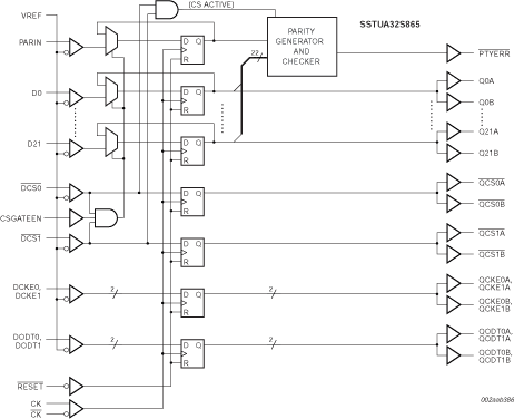
The SSTUA32S865 is a 1.8 V 28-bit 1 : 2 register specifically designed for use on two rank by four (2R x 4) and similar high-density Double Data Rate 2 (DDR2) memory modules. It is similar in function to the JEDEC-standard 14-bit DDR2 register, but integrates the functionality of the normally required two registers in a single package, thereby freeing up board real-estate and facilitating routing to accommodate high-density Dual In-line Memory Module (DIMM) designs.
The SSTUA32S865 also integrates a parity function, which accepts a parity bit from the memory controller, compares it with the data received on the D-inputs and indicates whether a parity error has occurred on its open-drain PTYERR pin (active LOW).
The SSTUA32S865 is packaged in a 160-ball, 12 x 18 grid, 0.65 mm ball pitch, thin profile fine-pitch ball grid array (TFBGA) package, which (while requiring a minimum 9 mm x 13 mm of board space) allows for adequate signal routing and escape using conventional card technology.
|
|
|
|
|
|
|
|---|---|---|---|---|---|
|
|
|
|
|
|
|
|
|
|
|
|
|
|
|
|
|
|
|
|
|
|
|
|
|
|
|
|
|
|
|
|
|
|
|
|
|
|
|
|
|
|
|
|
|
|
|
|
|
|
|
|
|
|
|
|
|
|
|
|
|
|
|
|
|
|
|
|
|
|
Quick reference to our documentation types
2 documents
Compact List
Receive the full breakdown. See the product footprint and more in the eCad file.
