Application Note (2)
Data Sheet (1)
-
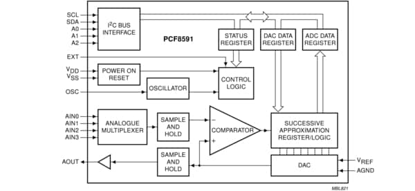
8-bit A/D and D/A converter[PCF8591]
The PCF8591 is a single-chip, single‑supply low‑power 8‑bit CMOS data acquisition device with four analog inputs, one analog output and a serial I²C‑bus interface. Three address pins A0, A1 and A2 are used for programming the hardware address, allowing the use of up to eight devices connected to the I²C‑bus without additional hardware. Address, control and data to and from the device are transferred serially via the two-line bidirectional I²C‑bus.
The functions of the device include analog input multiplexing, on-chip track and hold function, 8-bit analog‑to‑digital conversion and an 8‑bit digital‑to‑analog conversion. The maximum conversion rate is given by the maximum speed of the I²C-bus.
|
|
|
|
|
|
|
|---|---|---|---|---|---|
|
|
|
|
|
|
|
|
|
|
|
|
|
|
|
|
|
|
|
|
|
|
|
|
|
|
|
|
|
|
|
|
|
|
|
|
|
|
|
|
|
|
|
|
|
|
|
|
|
|
|
|
|
|
|
|
|
|
|
|
|
|
|
|
|
|
|
|
|
|
Quick reference to our documentation types
5 documents
Compact List
Receive the full breakdown. See the product footprint and more in the eCad file.
