BGS8L2 LTE LNA with bypass switch evaluation board

Roll over image to zoom in

Product Details

Supported Devices

RF

LNAs for LTE

Features

Power Management

  • The BGS8L2 is optimized for 728 MHz to 960 MHz
  • Supply voltage 1.5 V to 3.1 V
  • Optimized performance at low 5.2 mA supply current
  • Power-down mode current consumption < 1 µA
  • ESD protection on all pins (HBM > 2 kV)
  • Input and output DC decoupled

Size

  • 1.1 mm x 0.7 mm x 0.37 mm; 0.4 mm pitch: SOT1232
  • Noise figure (NF) = 0.9 dB
  • Gain 13 dB
  • Bypass switch insertion loss of 1.9 dB
  • High input 1 dB compression point of -1 dBm
  • High out of band IP3i of 1.5 dBm
  • Integrated temperature stabilized bias for easy design
  • Integrated matching for the output
  • 180 GHz transit frequency - SiGe:C technology

Buy Options

OM17005-Image

Click to expand

  • OM17005

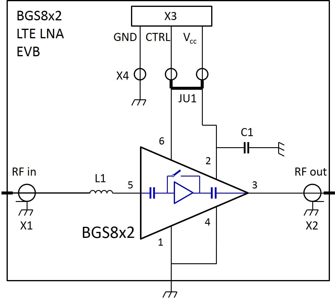
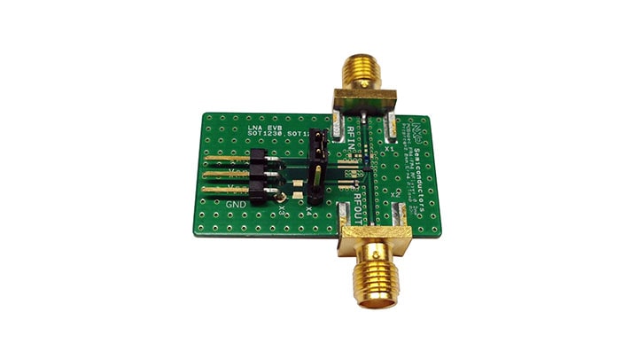
  • BGS8L2 LTE LNA with bypass switch evaluation board.

  • $160.00 USD
  • For a quantity of 1
Buy From Distributor

Design Resources

Select a section:

Design Files

1 design file

Support

What do you need help with?