Design Files
Receive the full breakdown. See the product footprint and more in the eCad file.
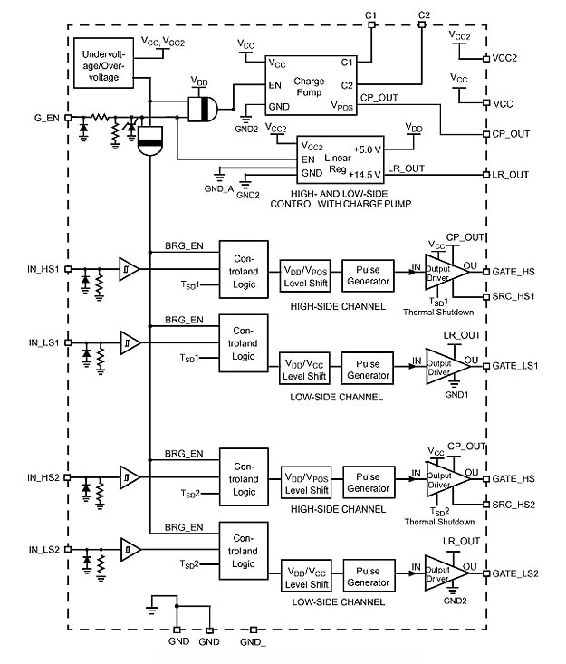
The NXP® MC33883 is an H-bridge gate driver (also known as a full-bridge pre-driver) IC with integrated charge pump and independent high and low side gate driver channels.

Note: To see the product features close this window.
Part numbers include: MC33883HEG.
|
|
|
|
|
|
|
|---|---|---|---|---|---|
|
|
|
|
|
|
|
|
|
|
|
|
|
|
|
|
|
|
|
|
|
|
|
|
|
|
|
|
|
|
|
|
|
|
|
|
|
|
|
|
|
|
|
|
|
|
|
|
|
|
|
|
|
|
|
|
|
|
|
|
|
|
|
|
|
|
|
|
|
|
Quick reference to our documentation types.
5 documents
Please wait while your secure files are loading.
Receive the full breakdown. See the product footprint and more in the eCad file.

Receive the full breakdown. See the product footprint and more in the eCad file.
1 hardware offering

1 hardware offering

To find additional partner offerings that support this product, visit our Partner Marketplace.
2 engineering services


There are no results for this selection.
To find additional partner offerings that support this product, visit our Partner Marketplace.