Analog Front End
NXP’s family of Analog front ends for industrial applications deliver high-performance data acquisition with benchmark accuracy and precision, enabling high-quality data capture for AI and ML workloads. Their universal and configurable input/output architecture allows a single device to support a broad range of measurement and control applications, while smart integration minimizes system BOM, reduces board space, and lowers the number of external components required.
Flexible calibration options support both plug-and-play pre-calibrated deployments and user-calibrated implementations, providing design flexibility across diverse use cases. In addition, these solutions are highly scalable, enabling hardware and software reuse across platforms to accelerate development and simplify product portfolios.
Advanced integrated diagnostics further enhance system resiliency, delivering robust system integrity and supporting functional safety (FuSA) requirements.
Input Analog Front End
Analog Front End Devices to measure voltage, current (4-20mA), RTD (PT100/PT1000), NTC/ PTC, Thermocouples, Load Cells.
NAFE13144
Universal ±25 V 4-Input Low Power AFE with Excitation source
16 bits.
NAFE11388
Universal ±25 V 8-Input Low Power AFE.
24 bits.
NAFE71388
High Speed Universal ±25 V 8-Input High Speed AFE.
24 bits.
NAFE73388
Universal ±25 V 8-Input High Speed AFE with excitation sources.
24 bits.
NAFE13388
Universal ±25 V 8-Input Low Power AFE with excitation sources.
24 bits.
NAFEB43388 new
Compact, 8-Input, 24 bits, Universal Fully Configurable Universal Analog Input AFE with Integrated DAC
Input and Output Analog Front End
Analog Front End Devices for Measuring Input / Driving Output (Integrated ADC and DAC)
NAFE33350 Fully Integrated Universal AO-AFE
Industrial-grade voltage/current AO-AFE, 18-bit resolution, high accuracy, fast dynamics, SW-configurable output.
Evaluation Boards and Reference Designs
NXP offers evaluation boards and reference designs that make secure edge solutions connected and efficient with innovative analog technologies. Start today.
Analog Front End FAQs
Learn more about NXP's N-AFE input analog front end portfolio of products.
What is the part family nomenclature for the NAFExx388 family?
Below is the nomenclature of the N-AFE family of devices:
| N-AFE | 1 | 3 | 3 | 8 | 8 |
|---|---|---|---|---|---|
|
1: Low power
7: High speed |
1: No VIEX
3: VIEX |
1: No Cal (calibrated)
3: Factory calibrated |
4: 16 bit
8: 24 bit |
4: 4-ch (channel)
8: 8-ch (channel) |
The low-power flavor has a max data rate of 288 ksps while the high-speed version can support up to 576 ksps in Normal Settling mode.
Refer to the data sheet or contact an NXP sales representative for available part numbers.
What are the different input ranges that N-AFE can measure?
The N-AFE has eight selectable PGA gain settings of 0.2 V/V to 16 V/V that provide eight differential input full-scale ranges from ±25 V to ±312.5 mV for a variety of applications. In general, all of the HV input characteristics are specified to the linear (nominal) input ranges for all of the channel gain settings, which is 80 % of the full input range.
| Nominal range values (V) | ||||||||
| Type | PGA gain setting | |||||||
| 0.2 | 0.4 | 0.8 | 1 | 2 | 4 | 8 | 16 | |
| Bipolar DIFF | ±20.00000 | ±10.00000 | ±5.00000 | ±4.00000 | ±2.00000 | ±1.00000 | ±0.50000 | ±0.25000 |
| Bipolar SE | ±10.00000 | ±5.00000 | ±2.50000 | ±2.00000 | ±1.00000 | ±0.50000 | ±0.25000 | ±0.12500 |
| Unipolar DIFF | ±10.00000 | ±5.00000 | ±2.50000 | ±2.00000 | ±1.00000 | ±0.50000 | ±0.25000 | ±0.12500 |
| Unipolar SE | ±10.00000 | ±5.00000 | ±2.50000 | ±2.00000 | ±1.00000 | ±0.50000 | ±0.25000 | ±0.12500 |
| Min and max values (V) | ||||||||
| Type | PGA gain setting | |||||||
| 0.2 | 0.4 | 0.8 | 1 | 2 | 4 | 8 | 16 | |
| Bipolar DIFF | ±25.00000 | ±12.50000 | ±6.25000 | ±5.00000 | ±2.50000 | ±1.25000 | ±0.62500 | ±0.31250 |
| Bipolar SE | ±12.50000 | ±6.25000 | ±3.12500 | ±2.50000 | ±1.25000 | ±0.62500 | ±0.31250 | ±0.15625 |
| Unipolar DIFF | ±12.50000 | ±6.25000 | ±3.12500 | ±2.50000 | ±1.25000 | ±0.62500 | ±0.31250 | ±0.15625 |
| Unipolar SE | ±12.50000 | ±6.25000 | ±3.12500 | ±2.50000 | ±1.25000 | ±0.62500 | ±0.31250 | ±0.15625 |
| Full range scale (V) | ||||||||
| Type | PGA gain setting | |||||||
| 0.2 | 0.4 | 0.8 | 1 | 2 | 4 | 8 | 16 | |
| Bipolar DIFF | 50 | 25 | 12.5 | 10 | 5 | 2.5 | 1.25 | 0.625 |
| Bipolar SE | 25 | 12.5 | 6.25 | 5 | 2.5 | 1.25 | 0.625 | 0.3125 |
| Unipolar DIFF | 25 | 12.5 | 6.25 | 5 | 2.5 | 1.25 | 0.625 | 0.3125 |
| Unipolar SE | 12.5 | 6.25 | 3.125 | 2.5 | 1.25 | 0.625 | 0.3125 | 0.15625 |
| Resolution (V) | ||||||||
| Type | PGA gain setting | |||||||
| 0.2 | 0.4 | 0.8 | 1 | 2 | 4 | 8 | 16 | |
| Bipolar DIFF | 3.0E-6 | 1.5E-6 | 745.1E-9 | 596.0E-9 | 298.0E-9 | 149.0E-9 | 74.5E-9 | 37.3E-9 |
| Bipolar SE | 3.0E-6 | 1.5E-6 | 745.1E-9 | 596.0E-9 | 298.0E-9 | 149.0E-9 | 74.5E-9 | 37.3E-9 |
| Unipolar DIFF | 3.0E-6 | 1.5E-6 | 745.1E-9 | 596.0E-9 | 298.0E-9 | 149.0E-9 | 74.5E-9 | 37.3E-9 |
| Unipolar SE | 3.0E-6 | 1.5E-6 | 745.1E-9 | 596.0E-9 | 298.0E-9 | 149.0E-9 | 74.5E-9 | 37.3E-9 |
How does the N-AFE implement cancelation of the wire resistance in a 3-wire RTD configuration?
Contrary to competitor solutions that implement two matched current generators to cancel the RTD wire resistance, the N-AFE utilizes the integrated current generator (VIEX) with low-temperature drift performance of 4 ppm/°C typical. The N-AFE optimizes the number of RTDs that can be connected to a single chip by using a single-current source allowing four 3-wire RTD measurements with a single chip.
What is the difference between user calibration and factory calibration?
The user calibration is the process by which the N-AFE is calibrated when it is already mounted on a PCB. The factory calibration is performed during chip manufacturing at the NXP factory. The user calibration achieves overall better accuracy with a typical TUE of ±0.002 % of full scale at room temperature. This is because all the errors introduced by external components and the soldering process are calibrated too. However, the accuracy guaranteed by the factory calibrated part, which is ±0.06 % of full scale at room, allows our customers to avoid the expensive and time-consuming calibration process if the provided accuracy fits their requirements.
Which register pointers should be used to utilize the factory calibration coefficients for NAFExx388?
The factory calibration is performed for all 8 PGA gain settings (input ranges) and the coefficients are stored in separate registers. Gain/OS coefficient pointer of 0, 1, 2, …, 7 should be used for Gain_code=0, 1, 2, …, 7 respectively for datasheet specified measurement accuracy. Please refer to Table 12 in the datasheet NAFE13388.
How fast can the N-AFE read in the Single-Channel Conversion mode?
The N-AFE is available in both a low-power (LP) version and a high-speed (HS) version with maximum data rates of 288 ksps and 576 ksps respectively. The single-channel conversion with normal settling provides the fastest readout of 3.472 us for the LP (NAFE1x388) version and 1.738 us for the HS (NAFE7x388) version.
How fast can the N-AFE read in Multichannel conversion mode?
When in Multichannel Conversion mode, the ADC input signal path requires 16.4 us and 8.2 us front-end settling time (defined as Tswitch in the EC table) for NAFE1x388 and NAFE7x388 respectively. The user should use single-cycle settling for multichannel readout to avoid settling errors. The ADC data rate in single-cycle settling mode is a quarter of the data rate in Normal Settling mode, for example, 72 ksps and 144 ksps for LP and HS parts respectively.
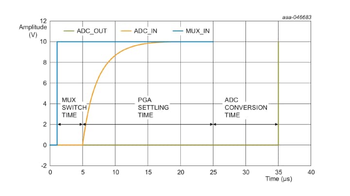
Code 17 for channel programmable delay meets the Tswitch requirement in both the low-power and high-speed flavors.
n channel read time = n * (Tcnv + Tch_delay)
where n = number of channels in multichannel read mode.
Tcnv = 1/DataRate
Tch_delay ≥ Tswitch.
The fastest readout for 8 inputs in Multichannel Conversion mode with single-cycle settling is:
NAFE1x388's fastest eight-channel read time = 8 * (13.88 us + 16.49 us) ≈ 240 us …..30 us/channel
NAFE7x388's fastest eight-channel read time = 8 * (6.94 us + 8.24 us) ≈ 120 us……….15 us/channel
How well can N-AFE reject 50/60 Hz line frequency?
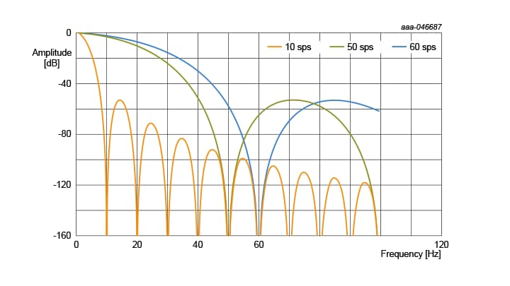
The NAFE13388 features a digital filter that provides a 50 Hz and 60 Hz Normal mode rejection (NMR) at lower data rates. The figure below shows the SINC4 filter NMR at the date rates of 10 sps, 50 sps and 60 sps.
What is the 50/60 Hz common-mode rejection (CMRR) at speeds higher than 100 sps?
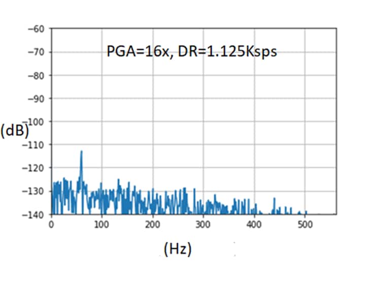
The N-AFE provides more than 110 dB CMRR at data rates much higher than 60 sps (without 50/60 Hz rejection of notch filter) as shown in the figure below.
What are the NAFExx388's Crosstalk (CT) specifications and conditions?
Static crosstalk: ±1 µV/V
Dynamic crosstalk (not AC spec): ±1 µV/V
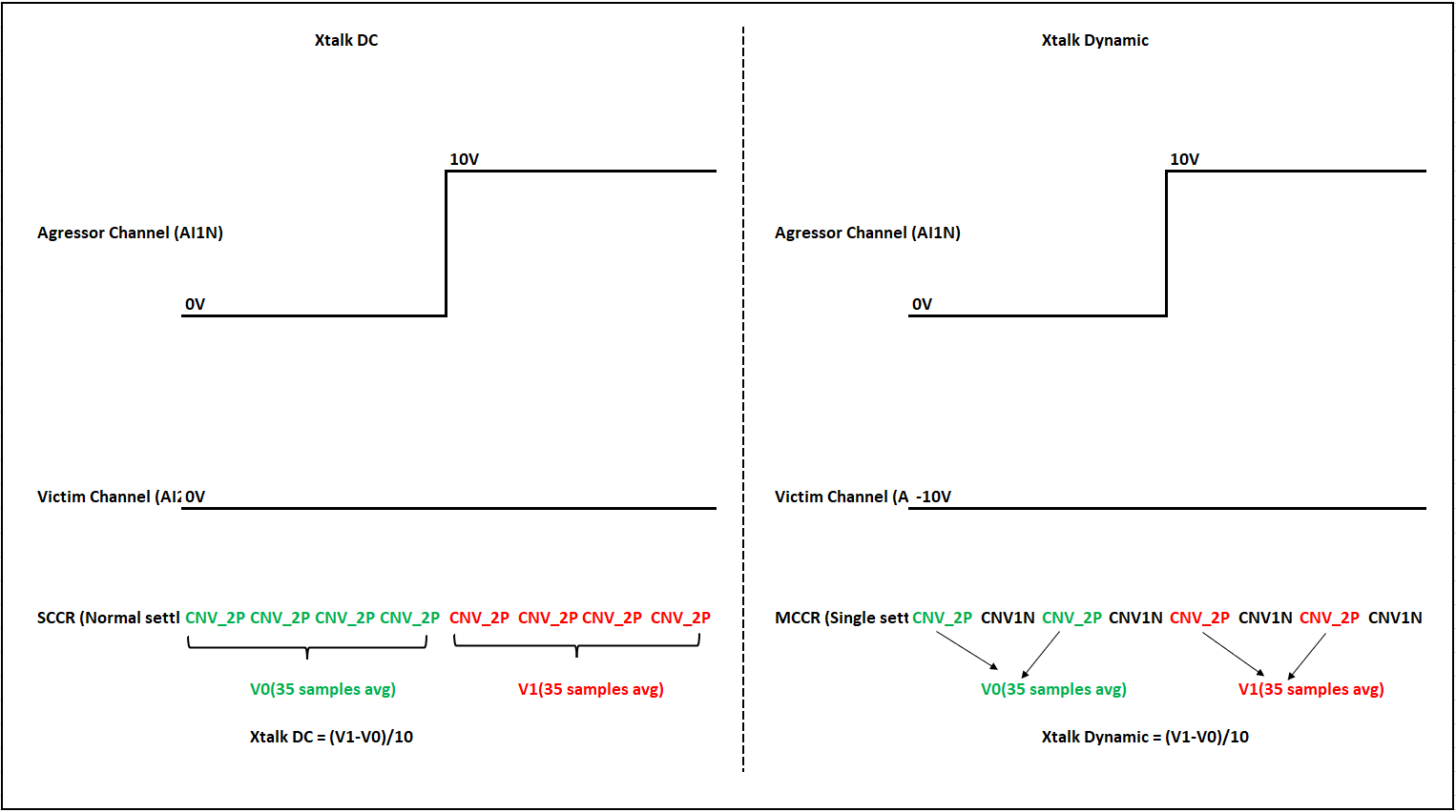
Below are the test conditions for crosstalk parameters:
-
Input crosstalk DC (single channel):
- Set the target channel at 0 V and vary the main channel from 0 V to 10 V
- This test uses single-channel conversion to see the impact of the main channel on the target channel
- The above procedure is repeated for the main channel varying from 0 V to -10 V
-
Input crosstalk dynamic (multichannel not an AC crosstalk):
- Set the target channel to -10 V and the adjacent main channel from 0 V to 10 V
- This test uses multichannel conversion to see the impact of the main channel on the target channel
- This quantifies the effect of the channel path settling (MUX+PGA) at specified DR0 and CH_delay in condition for a worst-case input swing at the ADC input
- The above procedure is repeated for the target channel at 10 V and the adjacent main channel varying from 0 V to -10 V
Learn more about NXP's N-AFE output analog front end portfolio of products.
What is the NAFE33352 and what are its primary applications?
The NAFE33352 is a software-configurable universal low-power Analog Input/Output Analog Front End (AIO-AFE) designed for high-precision measurement and control in industrial applications. It is used in PLCs, DCS I/O modules, data acquisition systems and industrial automation.
What types of analog signals can the NAFE33352 handle?
It supports voltage, current, resistance, temperature (RTD, thermocouple), load cell inputs and voltage and current outputs, with software-configurable ranges and modes.
What are the supported DAC output modes in the NAFE33352?
The DAC supports three output modes: High-Z mode, Voltage-output mode and Current-output mode. These are controlled via the AO_MODE register and associated control bits for enabling voltage or current source amplifiers.
What are the key features of the NAFE33352's ADC and DAC?
The device includes a 14/16/18-bit DAC and a 16/24-bit ADC. The ADC supports data rates from 7.5 sps to 288 ksps, and the DAC supports up to 100 ksps. It offers ±0.005 % ADC accuracy at room temperature and ±0.02 % over temperature.
What is the purpose of the Auto-DAC waveform generator?
The Auto-DAC waveform generator allows the device to autonomously generate waveforms (e.g., sine, triangle) based on user-defined amplitude, frequency and step size parameters. It is useful for test and calibration routines.
How does the NAFE33352 handle DAC slew rate control?
The device includes a programmable slew rate control feature that allows users to limit the rate of change of the DAC output. This is useful for avoiding overshoot or overcurrent in capacitive or inductive loads.
What calibration options are available for the NAFE33352?
The device supports both factory and user calibration. It includes non-volatile memory for storing calibration coefficients and allows self-calibration without external equipment.
Which register pointers should be used to utilize the factory calibration coefficients for Analog Output and Analog Input modes in NAFE33352?
The factory calibration is performed for all four modes of operations – Voltage Output, Current Output, Voltage Input and Current Input. These coefficients are stored in separate registers and in Table 39 from the NAFE33352 datasheet show their respective pointers.
How does the device ensure signal integrity and protection?
It includes low-drift voltage references, low-offset buffers, high-voltage amplifiers with 70 V input protection, and advanced diagnostic circuits for fault detection and predictive maintenance, which includes open/short detection, voltage rail monitoring, temperature sensing and programmable alarms for over/under range and overtemperature conditions.
How does the device handle protections when in output mode?
It features dual protection mechanisms for voltage and current output modes, including fast-reaction short-circuit protection and programmable overload protection with configurable thresholds and timers.
What are the thermal and electrical operating limits of the NAFE33352?
It operates from -40 °C to 125 °C, with a junction temperature limit of 150 °C. It supports ±36 V protection at the I/O terminals and has robust ESD ratings (HBM ±4500 V, CDM ±750 V).
What communication interface does the NAFE33352 use?
It uses a 4-wire SPI interface (CSB, SCLK, MOSI, MISO) with optional CRC for data integrity and speed up to 32 MHz It also includes SYNC and DRDY pins for synchronization and data readiness signaling.
How does the device support synchronization in multi-AFE systems?
The SYNC pin allows synchronization of multiple NAFE33352 devices. A rising edge on SYNC can trigger simultaneous conversions across devices, ensuring coherent sampling.
What are the available reading modes for data acquisition?
The NAFE33352 supports five reading modes: Single-Channel Single-Reading (SCSR), Single-Channel Continuous-Reading (SCCR), Multichannel Single-Reading (MCSR), Multichannel Multireading (MCMR), and Multichannel Continuous-Reading (MCCR).
How to debug a non-operational Analog Output in NAFE33352?
Use the following checklist to diagnose why the Analog Output (AO) is not functioning as expected:
- The REFDACBUF on NAFE33352 is disabled by default on power up. Enable it by setting AO_SYSCFG.DAC_SEL_REFBUF_ON=11\b. Without this, the DAC output will remain inactive
- When writing AO data over SPI, the device requires a minimum TDAC_wait time between the last SCLK edge and CSB rising edge. As shown in Figure 42 of the datasheet, this delay must be 18 system clock periods. For the NAFE33352, the system clock period is 217 ns, resulting in a TDAC_wait time of 3.9 µs. For the high speed NAFE93352, this wait time is half as long - 1.95 µs
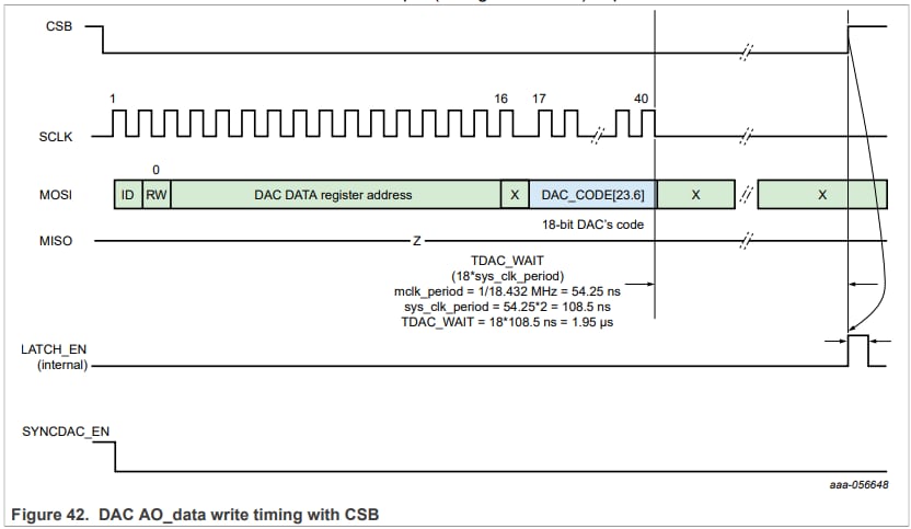
- Figure 42 also specifies that the 18 bit DAC code must be left aligned within the 24 bit SPI data frame. Misalignment will result in incorrect analog output
- Read the AIO_STATUS register to determine whether the device has detected: AO overload or AO short-circuit. If a fault is detected, the device forces AO_STATUS = Hi Z, placing the analog output in high impedance mode. To recover, perform a soft reset or hard reset after correcting the fault condition
What package and ordering options are available for the NAFE33352?
The device comes in a 6 mm x 6 mm 40-pin HVQFN package. Ordering options include reel and tray formats with part numbers like NAFE33352B40BSMP and NAFE33352B40BSE respectively.
Universal Fully Configurable Analog Input and Output Front End
Can be reconfigured to changing requirements in PLCs, remote I/O modules, process control systems, temperature measurement devices, load cells and other Industry 4.0 applications.
Design Resources
In this webinar we will discuss the challenges the designers face in developing a software-configurable universal analog input module and how the new NXP's N-AFE device is able to simplify the design.
Fully featured evaluation board for the NAFExx388 highly configurable AFE for industrial applications.
Additional Documents
N-AFE Universal Fully Configurable Analog Front End Family with Universal Analog Inputs Fact Sheet
N-AFE devices are highly configurable industrial-grade multichannel universal input analog front end (AFE) with high accuracy and precision for smart factories.
Read the fact sheetAdding Value to a PLC or Remote I/O Applications with the N-AFE Analog Front End Family
The N-AFE software configurable device adds value to PLC or remote I/O systems with high-precision measurement features. N-AFE analog front end enables the efficient design and enhanced reliability for industry 4.0 analog input applications.
Read the application noteIndustrial Application Measurements Using NXP AFE
This article discusses system-level implementation of voltage and current sensing, temperature and weight scale measurements, and system diagnostics using the NAFE13388EVB (evaluation board) and GUI.
Read the application noteNAFE Applications with MCUXpresso
This article introduces the precompiled NAFE software library for NXP proprietary MCUXpresso platform. The library consists of ready-to-use measurement script for the industrial applications (voltage, current, temperature and weight) with NAFE evaluation KIT as discussed in AN14102.
Read the application note