Getting Started with the KITVR55-FSSKTEVM
Contents of this document
-
Get Started
-
Get to Know the Hardware
-
Configure Hardware
-
Install Software
Sign in to save your progress. Don't have an account? Create one.
Purchase your KITVR55-FSSKTEVM | VR5500 Safety SBC Programming Board
1. Get Started
The NXP analog product development boards provide an easy-to-use platform for evaluating NXP products. The boards support a range of analog, mixed-signal and power solutions. They incorporate monolithic integrated circuits and system-in-package devices that use proven high-volume technology. NXP products offer longer battery life, a smaller form factor, reduced component counts, lower cost, and improved performance in powering state-of-the-art systems.
This page will guide you through the process of setting up and using the KITVR55- FSSKTEVM evaluation board.
1.1 Kit Contents/packing List
The KITVR55-FSSKTEVM contents include:
- Assembled and tested KITVR55-FSSKTEVM board in an anti-static bag
- 3.0 ft USB-STD A to USB-B-mini cable
- Two connectors, terminal block plug, 2 pos., str. 3.81 mm
- Three connectors, terminal block plug, 3 pos., str. 3.81 mm
- Jumpers mounted on board
- Quick start guide
1.2 Additional Hardware
In addition to the kit contents, the following hardware is necessary or beneficial when working with this kit.
- Power supply with a range of 8.0 V to 60 V and a current limit set initially to 1.0 A
1.3 Windows PC Workstation
This evaluation board requires a Windows PC workstation. Meeting these minimum specifications should produce great results when working with this kit.
- USB-enabled computer with Windows 7 or Windows 10
2. Get to Know the Hardware
2.1 Board features
- VBAT power supply connectors (Jack and Phoenix)
- VPRE output capability up to 1.0 A (socket limit) 3.3 V / 3.8 V / 4.1 V / 5.0 V
- VBUCK1/2 in Standalone mode (default) or Multiphase mode
- VBUCK3
- VBOOST 5.0 V or 5.74 V, up to 800 mA
- LDO1 and LDO2, from 1.1 V to 5.0 V, up to 400 mA
- Ignition key switch
- Embedded USB connection for easy connection to software GUI (access to I2C-bus, IOs, RSTB, INTB, Debug, MUX_OUT, regulators)
- LEDs that indicate signal or regulator status
- Support OTP fuse capabilities
- USB connection for register access, OTP emulation, and programming
- Voltage monitoring jumper setting
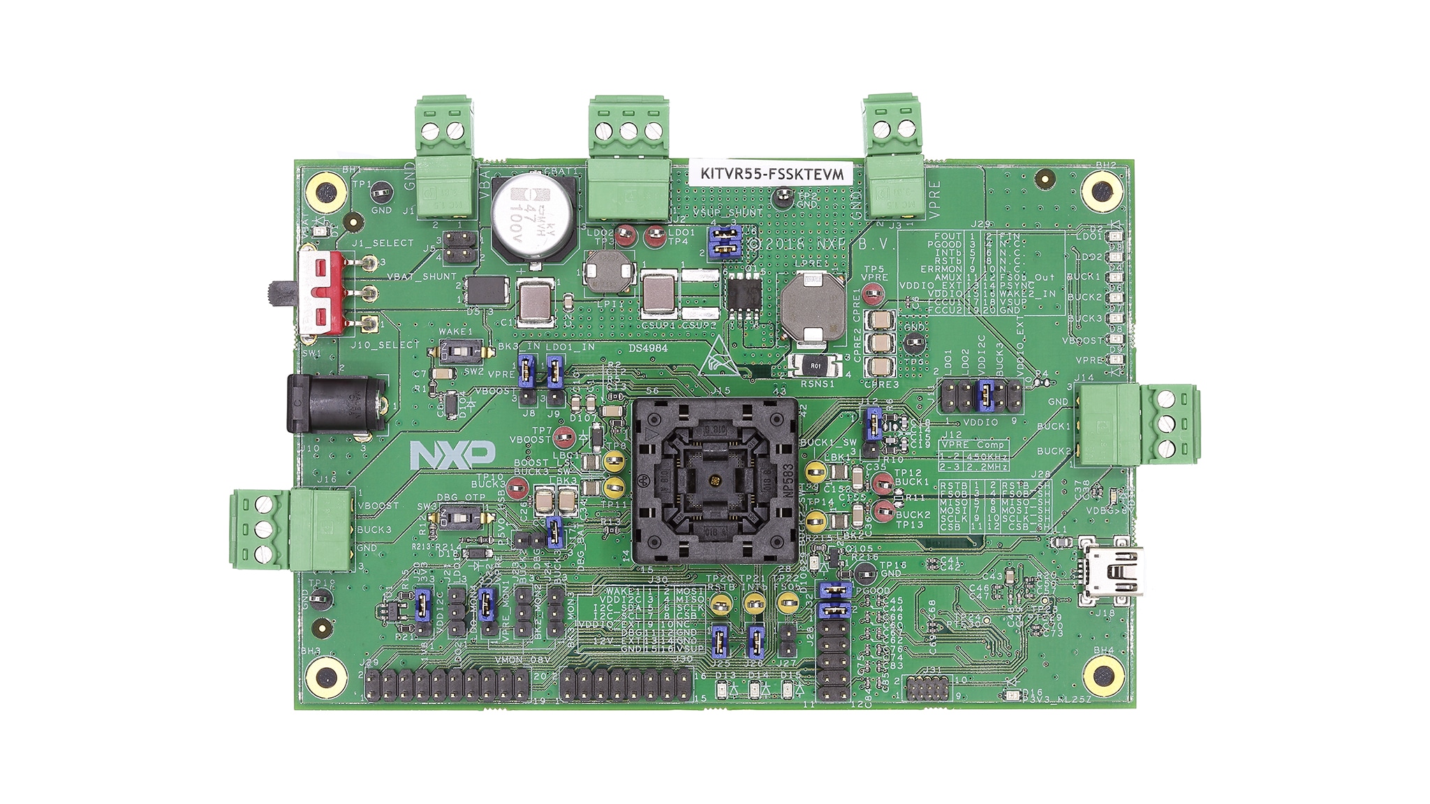
2.2 Board Description
The KITVR55-FSSKTEVM provides flexibility to play with all the features of the device and make measurements on the main part of the application. The KL25Z MCU installed on the board, combined with the FlexGUI software allows access to the registers in read and write mode. All regulators are accessible through connectors. Nonuser signal, like DC-to-DC switcher node is mapped on test points. Digital signals (SPI, I2C, RSTB, etc.) are accessible through connectors. Pin WAKE1 has a switch to control (ignition) them. A VBAT switch is available to power on or off the device.
The main purpose of this kit is to burn the OTP configuration. This kit can be operated in Emulation mode or in OTP mode. In Emulation mode, as long as the power is supplied, the board configuration stays valid. The OTP mode uses the fused configuration. The device can be fused three times. In OTP mode, the device always starts with the fused configuration, except if the user wants to overwrite OTP configuration using Emulation mode. This board is able to fuse the OTP without any extra tools or board.
2.3 Board Components
Overview of the KITVR55-FSSKTEVM evaluation board
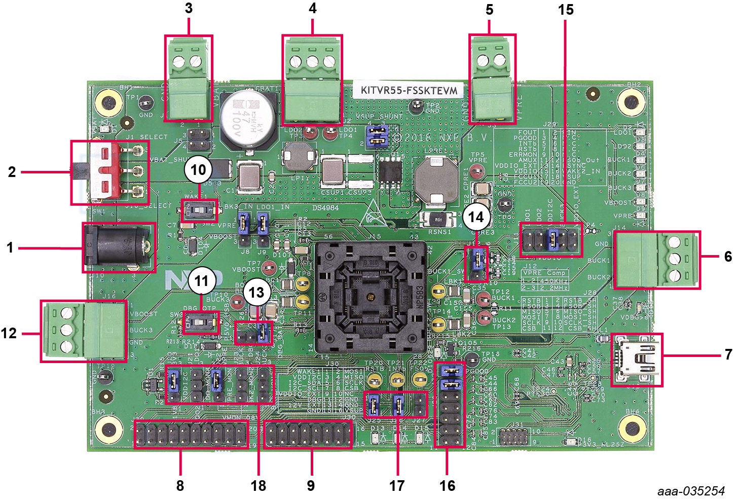
- VBAT Jack connector
- VBAT three position switch
- VBAT Phoenix connector
- LDO1/LDO2 power supplies
- VPRE power supply
- BUCK1/BUCK2 power supply
- USB connector (for FlexGUI control)
- Debug connectivity
- Programming
- WAKE1 switch
- OTP burning voltage switch
- VBOOST and BUCK3 power supply
- Debug voltage source
- Compensation network selection
- VDDIO selection
- RSTB connection to MCU
- RSTB and INTB signals
- VMON1 and VDDI2C selection
3. Configure Hardware
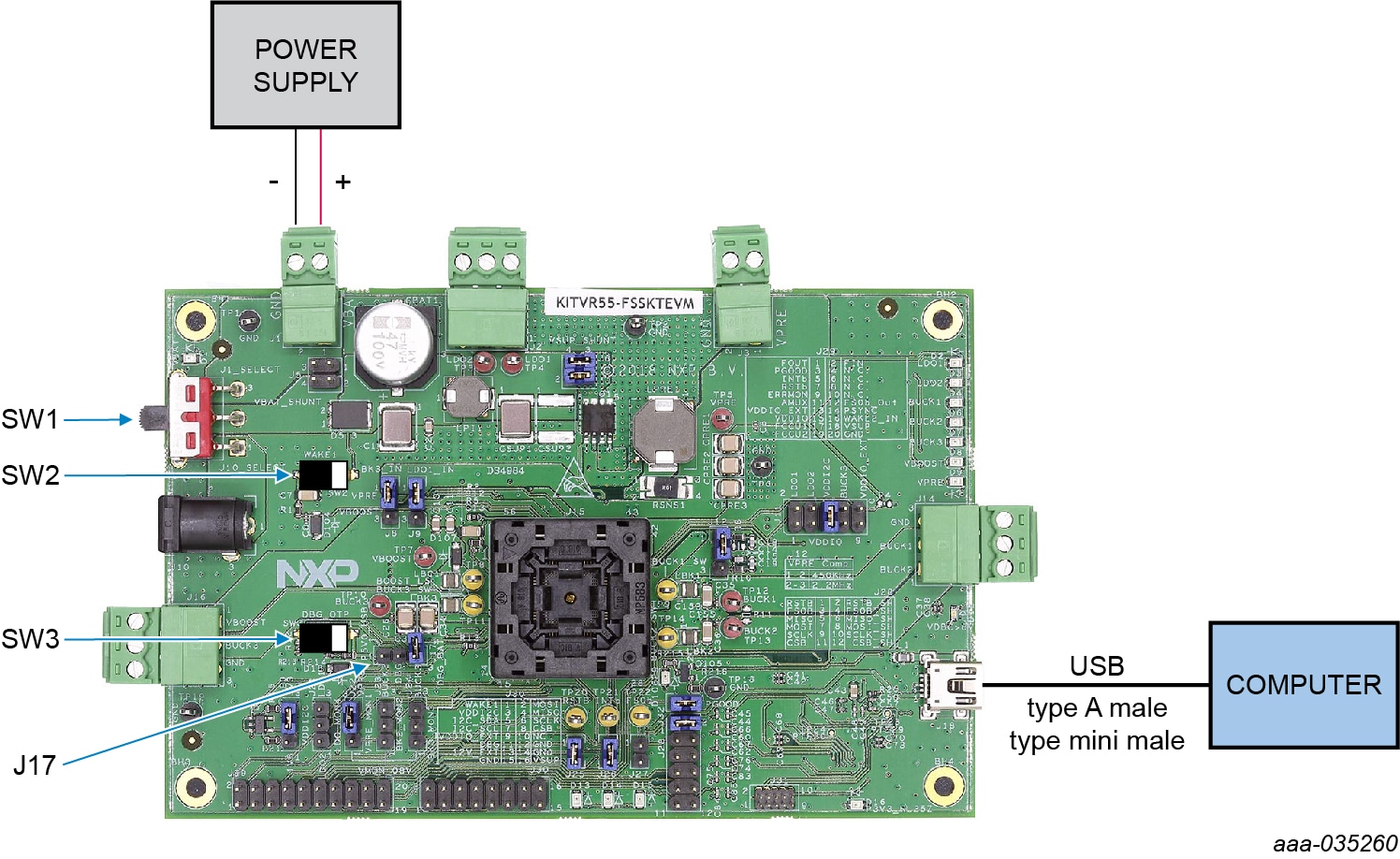
To configure the hardware, complete the following procedure:
-
Install jumpers for the configuration
Jumper Configuration J17connect 1-2 (connect 5.0 V on DBG pin from the USB) -
Configure switches
Switch Configuration SW1 middle position (VBAT off) SW2 open (WAKE1) SW3 open (OTP programming off) - Connect the Windows PC USB port to the KITVR55-FSSKTEVM development board using the provided USB 2.0 cable
- Set the DC power supply to 12 V and current limit to 1.0 A. With power turned Off, attach the DC power supply positive and negative output to KITVR55-FSSKTEVM VBAT Phoenix connector (
J1) - Turn on the power supply
- Close SW2
4. Install Software
4.2 Install FlexGUI Software Package
The FlexGUI software does not require any installation. Unzip the folder contents to a desired location on your computer.
- If necessary, install the Java JRE (Java SE Runtime Environment) available at JRE8 downloads and Windows 7 FlexGUI driver
- Download the latest FlexGUI (32-bit or 64-bit) version, available at VR5500 Safety SBC Programming Board
- Run the
flexgui-app-vr5500-fs5502.exefile - Restart the computer after successful download
Design Resources
Board Documents
Additional Resources
Product Summary Page
Tool Summary Page
The page provides overview information, technical and functional specifications, ordering information, documentation, and software. The Get Started provides quick-reference information applicable to using the KITVR55-FSSKTEVM board, including the downloadable assets.
References
In addition to our VR5500: High Voltage PMIC with multiple SMPS page, you may also want to visit:
Application pages:
- Automotive Vision Systems
- Mid to High Infotainment / eCockpit
- Entry Infotainment/Connected Radio
- Mid/High-End Infotainment Head Unit