Getting Started with the KITFS27SKTEVM Programming Board
Contents of this document
-
Out of the Box
-
Get Hardware
-
Configure Hardware
Sign in to save your progress. Don't have an account? Create one.
Purchase your KITFS27SKTEVM
1. Out of the Box
The NXP analog product development boards provide an easy-to-use platform for evaluating NXP products. The boards support a range of analog, mixed-signal and power solutions. They incorporate monolithic integrated circuits and system-in-package devices that use proven high-volume technology. NXP products offer longer battery life, a smaller form factor, reduced component counts, lower cost and improved performance in powering state-of-the-art systems.
This page guides you through the process of setting up and using the KITFS27SKTEVM programming board.
1.1 Kit Contents and Packing List
The kit contents include:
- Assembled and tested programming board and preprogrammed FRDM-KL25Z board in an antistatic bag
- 3.0 ft USB-STD A to USB-B-mini cable
- Six connectors, two-position terminal block plug, straight 3.81 mm
- Two connectors, three-position terminal block plug, straight 3.81 mm
- Jumpers mounted on board
- Quick Start Guide
1.2 Additional Hardware
In addition to the kit contents, the following hardware is necessary when working with this board.
- Power supply with a range of 8.0 V to 40 V and a current limit set initially to 1.0 A
1.3 Minimum System Requirements
This programming board requires a Windows PC workstation. Meeting these minimum specifications must produce great results when working with this evaluation board:
- USB-enabled computer with Windows 7, 10 or 11
1.4 Software
Installing software is necessary to work with this evaluation board. All listed software is available on the NXP GUI for Automotive PMIC Families information page or from our 'Secure Files' portal if the device is not in production.
2. Get Hardware
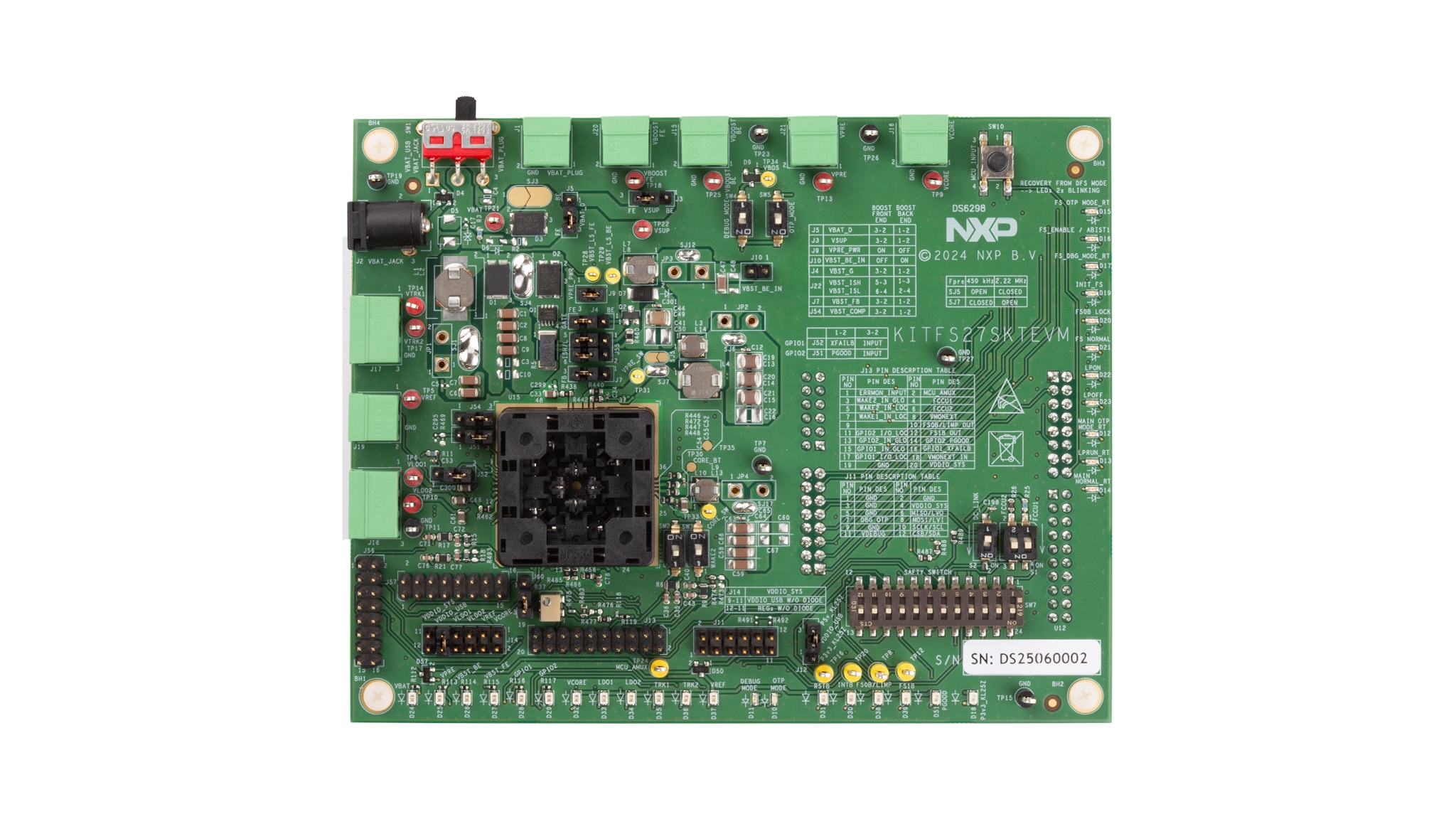
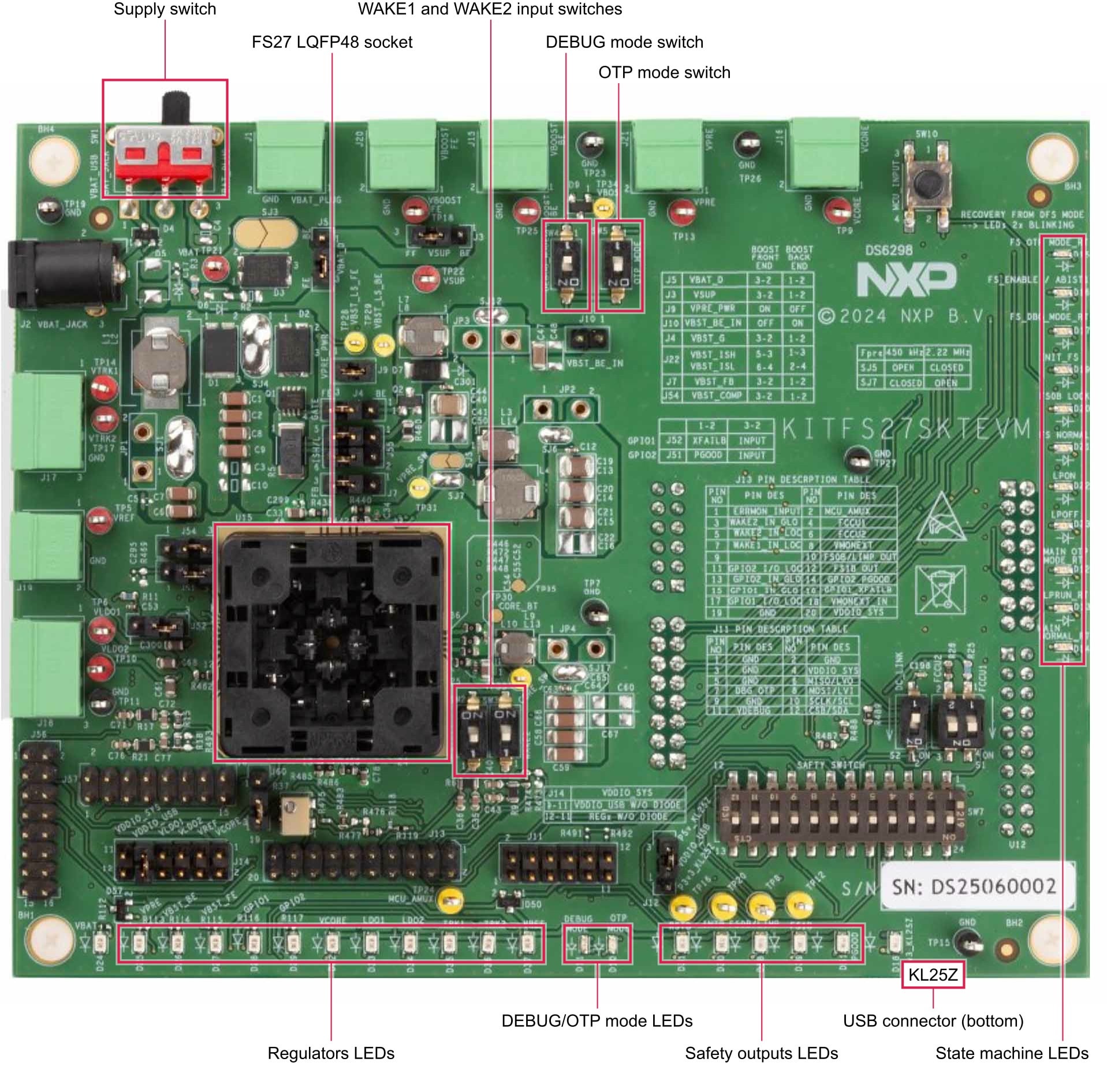
2.1 Board Features
VBATpower supply connectors (jack and Phoenix)LQFP48burn-in open-top socketBOOSTin independent mode or in front-end topology to support battery cranking profilesVPREoutput 5 V to 6.35 V, up to 2.5 A (limited to 1 A due to socket)VCOREoutput 0.8 V to 5.0 V, up to 3.5 A (limited to 2 A due to socket)LDO1andLDO2, from 1.0 V or 5.0 V, up to 400 mATRK1andTRK2, from 1.0 V or 5.0 V, up to 150 mAVREFaccuracy regulator for external ADC reference up to 80 mAFS0B/LIMP,FS1Bexternal safety pins- USB to SPI and I²C protocol for easy connection evaluation GUI
- LEDs that indicate signal or regulator status
- OTP fuse programming
- Advance system monitoring via
AMUX, and ADCs, and digital IOs - Analog variable resistor to test external
VMON
2.2 Board Description
The KITFS27SKTEVM provides the flexibility needed to play with all the features of the device and to take measurements in the main sections of the application. The FRDM-KL25Z board connected to the kit, combined with the FS27 NXP GUI for Automotive PMIC Families software, allows full configuration and control of the FS27 SBC. The LQFP48 socket on the board allows different samples to be tested or programmed.
An FS27 device must be inserted in the socket to enable OTP programming, emulation or evaluation. The performance on this board is limited; for further evaluation, another board must be required - check options on FS2700.
3. Configure Hardware
3.1 Install Software
The software tools are available on NXP GUI for Automotive PMIC Families or from our 'Secure Files' portal if the device is not in production.
3.2 Default Board Configuration
The kit is provided with a default board configuration following the legend on Figure 2.
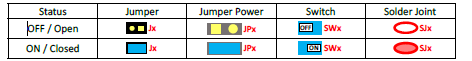
The default board configuration shown in Figure 3 is suited for a boost in front-end topology.
SJ15 and SJ18 are on the bottom.
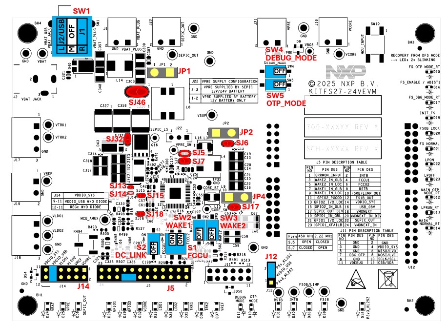
| Schematic Label | Description | Default Setting |
|---|---|---|
JP1 |
BOOST front-end regulator input inductor current measurement |
Open |
JP2 |
VPRE regulator output inductor current measurement |
Open |
JP3 |
BOOST regulator back-end input inductor current measurement |
Open |
JP4 |
VCORE regulator output inductor current measurement |
Open |
J3 |
VSUP selector (BOOST FE/BE) |
3 to 2 |
J4 |
VBST_G selector (BOOST FE/BE) |
3 to 2 |
J5 |
VBAT_D selector (BOOST FE/BE) |
3 to 2 |
J7 |
VBST_FB selector (BOOST FE/BE) |
3 to 2 |
J9 |
VPRE_PWR (BOOST FE/BE) |
ON |
J10 |
VBST_IN_BE (BOOST FE/BE) |
OFF |
J54 |
VBST_COMP selector (BOOST FE/BE) |
3 to 2 |
J55 |
VBST_ISH and VBST_ISL selectors (BOOST FE/BE) |
3 to 5 and 4 to 6 |
JP1 |
BOOST front-end regulator input inductor current measurement |
OFF |
JP2 |
VPRE regulator output inductor current measurement |
OFF |
JP3 |
BOOST regulator back-end input inductor current measurement |
OFF |
JP4 |
VCORE regulator output inductor current measurement |
OFF |
SJ1 |
Bypass JP1: jumper for BOOST front-end regulator input inductor current measurement |
Closed |
SJ3 |
Bypass D3: VBAT reverse protection diode | Open |
SJ4 |
Bypass D2: VBAT reverse protection diode when BOOST front-end |
Closed |
SJ6 |
Bypass JP2: jumper for VPRE regulator output inductor current measurement |
Closed |
SJ7 |
Connect VPRE_SW to L4 (inductor FPRE = 455 kHz) |
Closed |
SJ12 |
Bypass JP3: jumper for BOOST back-end regulator input inductor current measurement |
Closed |
SJ17 |
Bypass JP4: jumper for VCORE regulator output inductor current measurement |
Closed |
SJ15 |
Connect VPRE regulator output to TRKIN pin |
Closed |
SJ18 |
Connect VPRE regulator output to LDOIN pin |
Closed |
SW1 |
VBAT supply | 2 (middle) |
SW2 |
WAKE1 switch global |
OFF |
SW3 |
WAKE2 switch global |
OFF |
SW4 |
Debug mode | OFF |
SW5 |
Overtemperature protection (OTP) mode | OFF |
SW7 |
Safety switch (breaker) | All ON |
SW8 |
Communication protocol manual switch | OFF |
SW9 |
Communication interface switch (breaker) | All ON |
SW11 |
LED switch (breaker) | All ON |
S1 |
Fault collection and control unit (FCCU) switch | All ON |
S2 |
Direct current (DC) link switch | OFF |
3.3 LQFP48 Open Top Socket
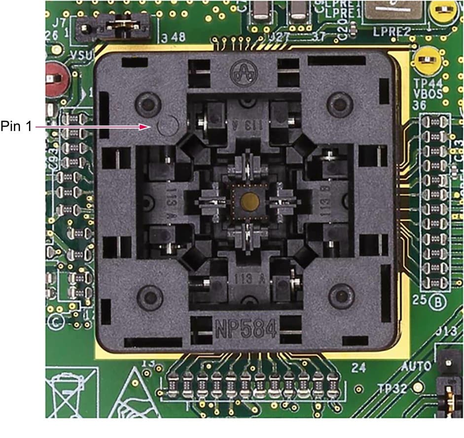
This KIT is equipped with an LQFP48 open socket. This socket enables FS27 family OTP emulation and OTP programming on several samples with easy insertion or replacement. The socket part number is NP584-048-113 Yamaichi (maximum current per pin 1 A).
To insert or change a device, the user must push the top of the socket and keep it pressed, then carefully insert the IC with pins correctly aligned. Pin 1 is on the top left of the socket.
Design Resources
Board Documents
Available to selected customers only a nondisclosure agreement (NDA) is required. Contact your local NXP sales representative for more information.
Additional References
In addition to the FS27, 12 V / 24 V / 48 V Safety System Basis Chip for ASIL D, visit: