Getting Started with the KITPF5300SKTEVM Evaluation Board
Contents of this document
-
Out of the Box
-
Get Hardware
-
Configure Hardware
Sign in to save your progress. Don't have an account? Create one.
Purchase your KITPF5300SKTEVM
1. Out of the Box
The NXP analog product development boards provide an easy-to-use platform for evaluating NXP products. The boards support a range of analog, mixed-signal and power solutions. They incorporate monolithic integrated circuits and system-in-package devices that use proven high-volume technology. NXP products offer longer battery life, a smaller form factor, reduced component counts, lower cost and improved performance in powering state-of-the-art systems.
This page will guide you through the process of setting up and using the KITPF5300SKTEVM board.
1.1 Kit Content and Packing List
The KITPF5300SKTEVM kit contents include:
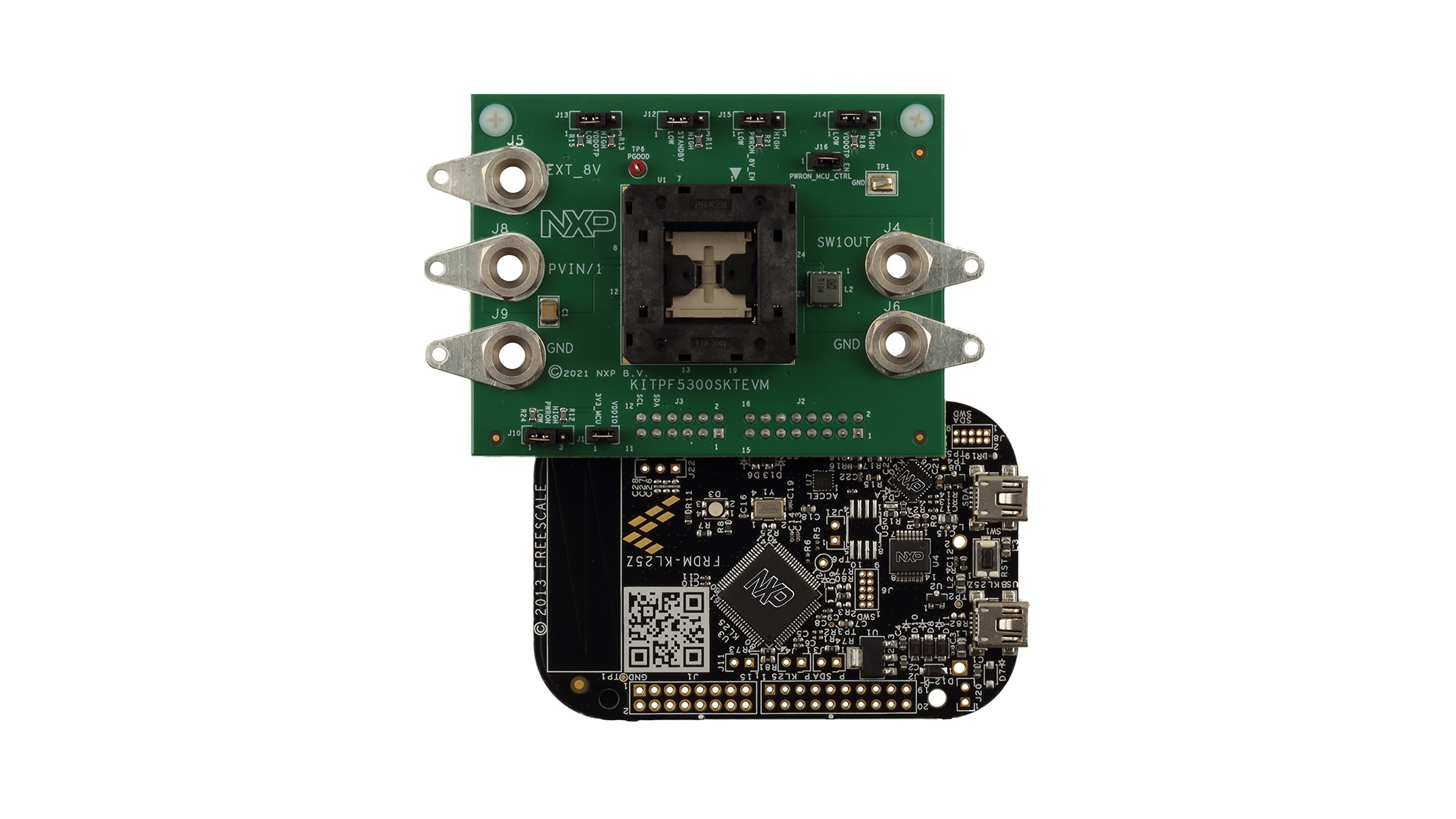
- Assembled and tested evaluation board and preprogrammed FRDM-KL25Z microcontroller
- 3.0 ft USB-STD A to USB-B-mini cable
- Jumpers mounted on board
1.2 Software
The software listed here must be installed before working with this evaluation board.
- NXP GUI installation package
2. Get Hardware
2.1 Board Features
- VIN and PVIN connectors
- SW1 output capability up to 15 A
- Load slammer connector
- PGOOD output
- Emulation mode capabilities
- USB connection and GUI for register access, OTP emulation and programming
2.2 Bundle Description
The KITPF5300SKTEVM provides a way to OTP program the PF5300 and conduct basic power-up testing of a programmed part. Loading of the DC-DC converter is not allowed.
2.3 Bundle Components

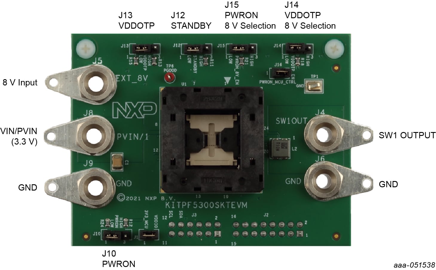
Table 1. Board description
| Position | Function | Description |
|---|---|---|
J5 |
EXT_8V | 8.0 V supply input needed for OTP programming |
J8 |
VIN / PVIN | Input power supply (3.3 V) |
J9, J6 |
GND | Ground |
J4 |
Output voltage | Output voltage |
J12 |
STANDBY | 1-2: Default. STANDBY = GND 2-3: STANDBY = VDDIO |
J10 |
PWRON Functional control |
Open: Default. PWRON controlled through J16. 1-2: PWRON = GND 2-3: PWRON = VDDIO Use only if J16 is open. |
J13 |
VDDOTP configuration | Open: Default. Use for OTP programing. 1-2: Connect to ground. 2-3: Pull up to VDDIO. Use if trying XFAILB functionality. |
J4 |
VDDOTP 8V selection | 1-2: Do not apply EXT_8V to VDDOTP/XFAILB pin 2-3: Default. Apply 8V_EXT to VDDOTP/XFAILB pin Open: If evaluating XFAILB functionality |
J5 |
PWRON configuration | Control PWRON voltage in relation to EXT_8V 1-2: Apply EXT_8V/2 to PWRON pin 2-3: Default. Apply EXT_8V to PWRON pin |
J6 |
PWRON connectivity | Open: PWRON controlled by J10 Closed: Default. PWRON controlled by J15/MCU. |
J1 |
VDDIO supply | Closed: Default |
3. Configure Hardware
3.1 Configure the Hardware
Once the user has installed the NXP GUI, follow these instructions to quickly power up the board.
Powering up the board with pre-programmed OTP configuration:
- Make sure that the board has the right jumper configuration.
- Ensure that
SW4is in the NORMAL position. - Verify that the FRDM-KL25Z microcontroller is plugged in, and the USB cable on the FRDM-KL25Z microcontroller connector side is attached. It is important that the USB cable is connected to a PC because the cable enables communication with the NXP GUI and provides the VDDIO reference for the IC.
- Apply VIN and PVIN with PWRON = 0.
- Move
J10from 1-2 to 2-3 to turn on the PF53. - Open the GUI and communicate as required.
Powering up the board in Debug mode:
Debug mode allows the user to modify OTP mirror registers before powering up. This facilitates exercising different features of the PF5300 while deciding on the best configuration for a given application.
- Ensure that jumpers in the board are configured.
- Connect the FRDMKL25Z board to the socketed board.
- Connect the mini-USB cable from the USB port of the KL25Z to the PC that runs the GUI.
- Apply 8.0 V to the EXT_8V connector
J5. - Apply 3.3 V to the VIN/PVIN connector
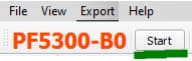
J8. - Open the GUI and click Start in the top-left.
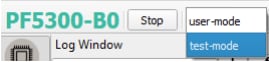
- Select Test Mode from the menu selection as shown below, then click Apply.
- Go to the PROG tab in the left side selection.
- Select the programming source – either from a script file, or to use the existing GUI configuration.
- Click the Program button to program the OTP fuses with the selected configuration.
Design Resources
Board Information
Additional References
In addition to our PF53, 12 A/8 A/15 A Core Supply Regulator with AVP and Watchdog page, you may also want to visit: