Getting Started with the NVT4558-4858-EVB Evaluation Board
Contents of this document
-
Out of the Box
-
Get Hardware
-
Configuring Hardware
Sign in to save your progress. Don't have an account? Create one.
Purchase your NVT4558-4858-EVB | SD/SIM Level Shifter Evaluation Board
1. Out of the Box
The NXP analog product development boards provide an easy-to-use platform for evaluating NXP products. The boards support a range of analog, mixed-signal and power solutions. They incorporate monolithic integrated circuits and system-in-package devices that use proven high-volume technology. NXP products offer longer battery life, a smaller form factor, reduced component counts, lower cost, and improved performance in powering state-of-the-art systems.
This page will guide you through the process of setting up and using the NVT4558-4858-EVB board.
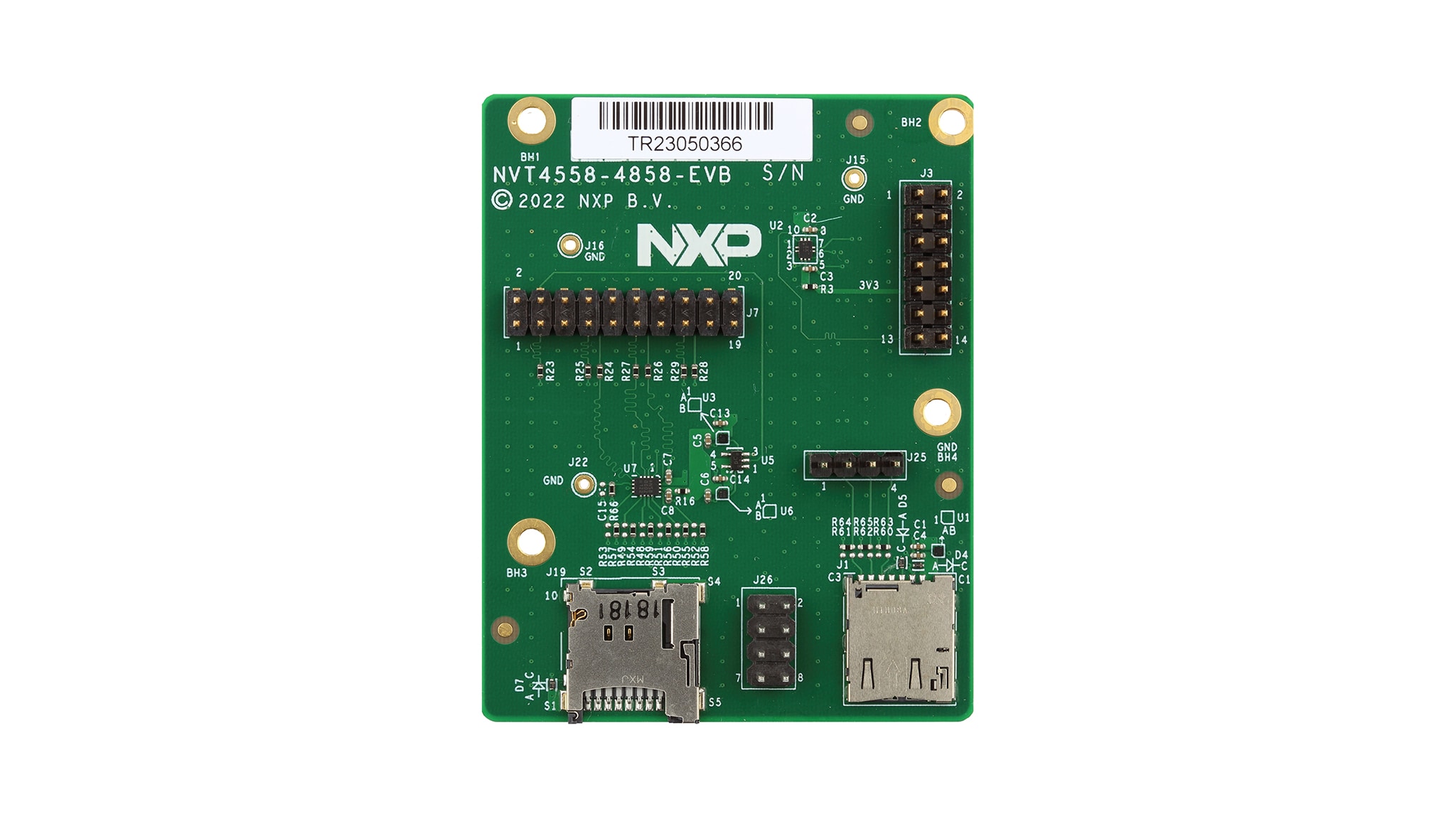
1.1 Kit Content and Packing List
The NVT4558-4858-EVB kit contents include:
- Assembled and tested evaluation board in an anti-static bag
1.2 Additional Hardware
In addition to the kit contents, the following hardware is necessary or beneficial when working with this reference board:
- Signal generator
- Oscilloscope
- Voltmeter
- Triple power supplies – 1V8, 3V3, Variable (1V0 - 3V3)
2. Get Hardware
2.1 Board Features
- Installed NVT4858
- Installed NVT4558
- Installed micro-SD card socket
- Installed SIM card socket
- SD/SIM input headers
- SD/SIM output headers
- 1V8/3V3 switchable SD card power circuit
- SD/SIM card power On/Off switch
2.2 Board Description
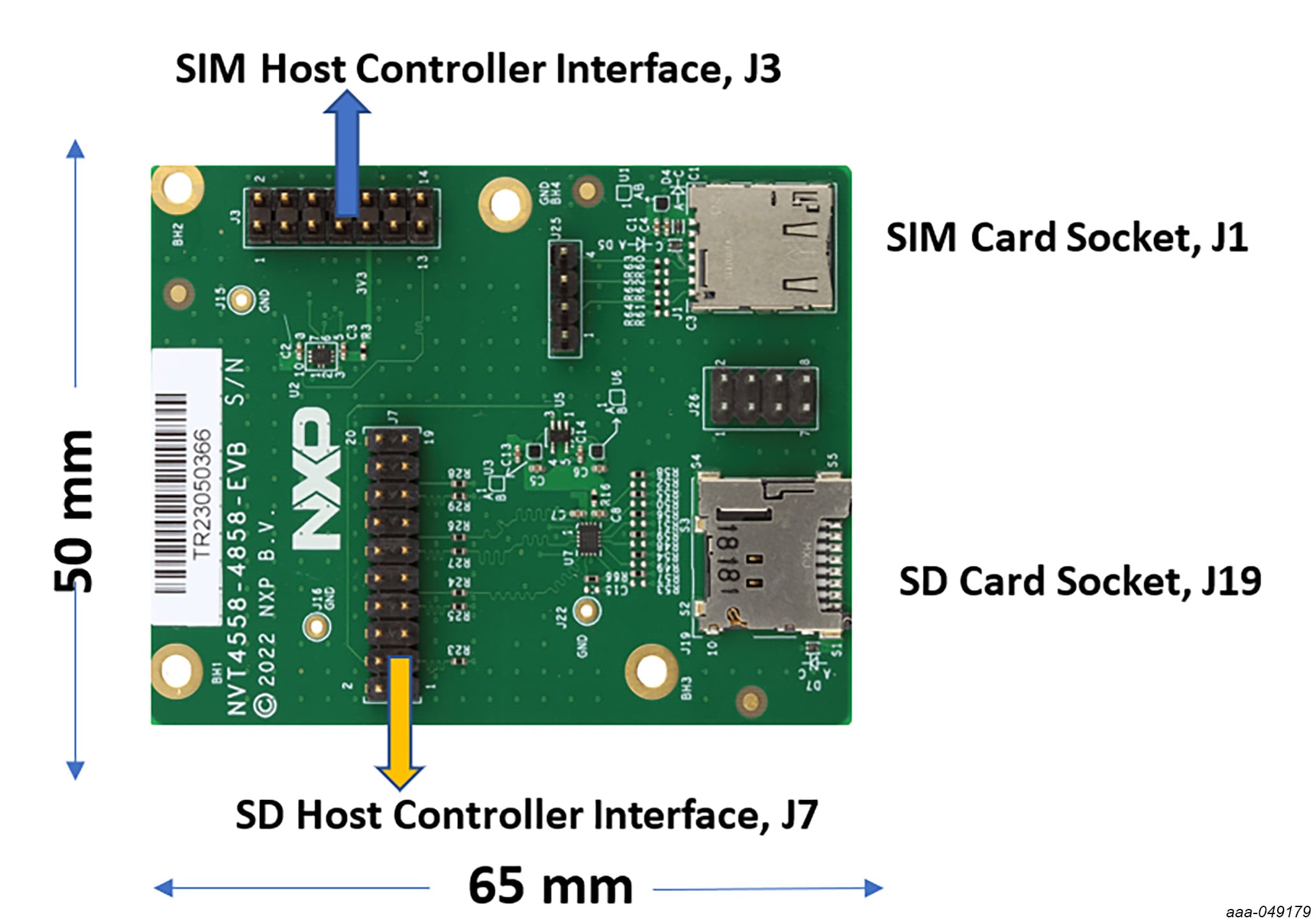
As default, NVT4558-4858-EVB evaluation board is loaded with the NVT4858 (SD level shifter) as well as the NVT4558 (SIM level shifter) along with one SD card socket and one SIM card socket.
There are two 100 mil headers that allow system platform with SD/SIM controller to take direct control of the SD and the SIM level shifters as well as SD and SIM cars sockets. The factory default setup is to bring the SD/SIM interface to the output headers, but by changing the optional configuration resistors the SD/SIM output can be brought to the SD/ SIM sockets.
3. Configuring Hardware
The demo board is designed to be a stand-alone board to allow the users to evaluate the performance of the NVT4858 or the NVT4558. There are four 100 mil headers, and the connections to all of the pins of the NVT4858 and the NVT4558 are available at these headers. In addition, there is one SIM card socket and one SD card socket available on the board. The SIM card, or the SD card that is inserted in the socket can be directly accessed by the SD host controller or the SIM controller via the 100 mil headers on the host interface side of the level shifter.
3.1 NVT4858 Example Evaluation Setup (VCCA = 1V2, VCCB = 3V3)
- Apply 1.2 V to VCCA (
J27pin 18) - Apply 1.8 V to SD_VDD_1V8 (
J27pin 20) - Apply 3.3 V to SD_VDD_3V3 (
J27pin 19) - Apply 1.2 V to SDPWR_3V3_n1V8 (
J27pin 4) to set VCCB to 3V3 - Apply a 1.2 V clock up to 200 MHz to NVT4858 (U7) host side via
J7 - The corresponding 3.3 V clock should be output on the SD card side and can be scoped on
J26.
3.2 NVT4558 Example Evaluation Setup (VCCA = 1V2, VCCB = 3V3)
- Apply 1.2 V to VCCA (
J3pin 2) - Apply 3.3 V to VCCB (
J3pin 9) - Apply 1.2 V to EN pin (
J3pin 13) to enable NVT4558 - Apply a 1.2 V clock up to 10 MHz to NVT4558 (U2) host side via
J3 - The corresponding 3.3 V clock should be output on the SIM card side, and can be scoped on
J25.
Design Resources
Board Information
Additional References
In addition to our NVT4858, SD, SDIO, Mini SD, Micro SD and SIM Card Voltage Level Translator with EMI Filter and ESD Protection page, you may also want to visit: