Getting Started with the P3A9606-EVB Evaluation Board
Contents of this document
-
Out of the Box
-
Get Hardware
-
Configure Hardware
Sign in to save your progress. Don't have an account? Create one.
Purchase your P3A9606JK-EVB 2-Channel Translator EV Board
1. Out of the Box
The NXP analog product development boards provide an easy-to-use platform for evaluating NXP products. The boards support a range of analog, mixed-signal and power solutions. They incorporate monolithic integrated circuits and system-in-package devices that use proven high-volume technology. NXP products offer longer battery life, a smaller form factor, reduced component counts, lower cost, and improved performance in powering state-of-the-art systems.
This page will guide you through the process of setting up and using the P3A9606JK-EVB evaluation board.
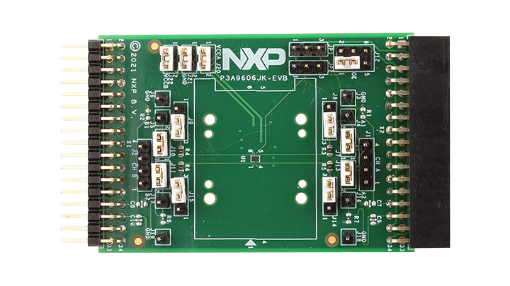
1.1 Kit Contents and Packing List
The P3A9606JK-EVB contents include:
- Assembled and tested evaluation board in an anti-static bag
- Quick Start Guide
This product has not undergone formal EMC assessment. It is the responsibility of the user to ensure that any finished assembly complies with applicable regulations on EMC inter ference. EMC testing, and other testing requirements for CE is the responsibility of the user.
1.2 Additional Requirements
- External power supplies as VCCA and VCCB
- External signal generator or signal(s) to be shifted from the host system
- Scope to observe the shifted signal(s)
2. Get Hardware
2.1 Board Features
- 2-bit, dual supply level shifter with auto sensing
- VCCA can be between 0.7 V to 1.98 V, and VCCB can be between 0.7 V to 1.98 V
- Signals to be shifted are to be connected to A2/A1 or B2/B1 and the shifted signals are available on B2/B1 or A2/A1
2.2 Board Description
P3A9606JK can be used as a standalone level shifter when a CERES is not available for evaluation and testing. The user can manually connect the signals to be shifted to port A1/A0 and B1/B0 of the P3A9606JK. External VCCA/VCCB can be manually selected and connected to the evaluation board.
As default, P3A9606JK-EVB evaluation board is configured (with jumper settings) to be mated to a CERES motherboard serial expansion bus as a level shifter on the SPI bus. If needed, P3A9606JK-EVB evaluation board can be bypassed using jumper settings to remove it from the SPI bus.
The evaluation boards are shipped with a P3A9606JK soldered on as U1; a socket (U2 on the
schematic) can be used in place of U1 to allow the user the flexibility of repeatedly replacing
P3A9606JK multiple times. U1 and U2 share the same PCB footprint, therefore, U1 must be removed
first before U2 as a socket can be installed.
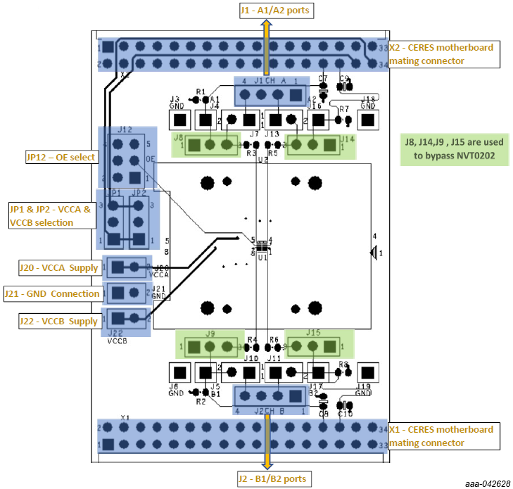
3. Configure Hardware
3.1 Configure the Hardware
- Connect VCCA to
J20 - Connect VCCB to
J22 - Use
JP12to enable P3A9606 - Connect signals to be shifted to A2 (
J14) and A1 (J8) - Power up VCCA and VCCB
- The shifted signals can be observed at B2 (
J15) and B1 (J9)
Design Resources
Board Information
Additional References
In addition to our P3A9606, Dual bidirectional I3C/I²C-bus and SPI voltage-level translator, you may also want to visit:
- Voltage Level Translator pages: NTB0104, PCA9306
- Hardware pages: Analog toolbox