Application Note (7)
Data Sheet (1)
Errata (3)
-
LPC915 Erratasheets[ES_LPC915]
-
LPC917 Erratasheets[ES_LPC917]
-
LPC916 Erratasheets[ES_LPC916]
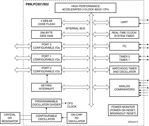
The P89LPC915/916/917 are single-chip microcontrollers, available in low-cost packages, based on a high performance processor architecture that executes instructions in two to four clocks, six times the rate of standard 80C51 devices. Many system-level functions have been incorporated into the P89LPC915/916/917 in order to reduce component count, board space, and system cost.
Additional features
|
|
|
|
|
|
|
|---|---|---|---|---|---|
|
|
|
|
|
|
|
|
|
|
|
|
|
|
|
|
|
|
|
|
|
|
|
|
|
|
|
|
|
|
|
|
|
|
|
|
|
|
|
|
|
|
|
|
|
|
|
|
|
|
|
|
|
|
|
|
|
|
|
|
|
|
|
|
|
|
|
|
|
|
Quick reference to our documentation types
1-10 of 14 documents
Compact List
1 design file
Receive the full breakdown. See the product footprint and more in the eCad file.