
Application Note (2)
-
AN10579[AN10579]
Brochure (4)
-
LED Drivers Selector Guide[LED-DRIVER-SELECTOR-GUIDE]
Data Sheet (1)
-
4-bit Fm+ I2C-bus LED driver[PCA9633]
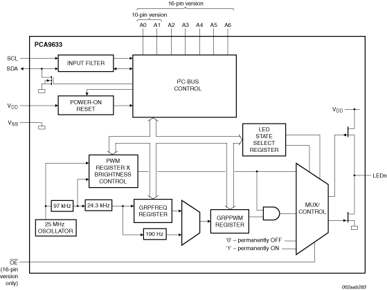
The PCA9633 is an I²C-bus controlled 4-bit LED driver optimized for Red/Green/Blue/Amber (RGBA) color mixing applications. Each LED output has its own 8-bit resolution (256 steps) fixed frequency Individual PWM controller that operates at 97 kHz with a duty cycle that is adjustable from 0 pct to 99.6 pct to allow the LED to be set to a specific brightness value. A fifth 8-bit resolution (256 steps) Group PWM controller has both a fixed frequency of 190 Hz and an adjustable frequency between 24 Hz to once every 10.73 seconds with a duty cycle that is adjustable from 0 pct to 99.6 pct that is used to either dim or blink all LEDs with the same value.
Each LED output can be off, on (no PWM control), set at its Individual PWM controller value or at both Individual and Group PWM controller values. The LED output driver is programmed to be either open-drain with a 25 mA current sink capability at 5 V or totem pole with a 25 mA sink, 10 mA source capability at 5 V. The PCA9633 operates with a supply voltage range of 2.3 V to 5.5 V and the outputs are 5.5 V tolerant. LEDs can be directly connected to the LED output (up to 25 mA, 5.5 V) or controlled with external drivers and a minimum amount of discrete components for larger current or higher voltage LEDs.
The PCA9633 is one of the first LED controller devices in a new Fast-mode Plus (Fm+) family. Fm+ devices offer higher frequency (up to 1 MHz) and more densely populated bus operation (up to 4000 pF).
The active LOW Output Enable input pin (OE) allows asynchronous control of the LED outputs and can be used to set all the outputs to a defined I²C-bus programmable logic state. The OE can also be used to externally PWM the outputs, which is useful when multiple devices need to be dimmed or blinked together using software control. This feature is available for the 16-pin version only.
Software programmable LED Group and three Sub Call I²C addresses allow all or defined groups of PCA9633 devices to respond to a common I²C address, allowing, for example, all red LEDs to be turned on or off at the same time or marquee chasing effect, thus minimizing I²C-bus commands.
The PCA9633 is offered with 3 different I²C-bus address options: fixed I²C-bus address (8-pin version), 4 different I²C-bus addresses from 2 programmable address pins (10-pin version), and 126 different I²C-bus addresses from 7 programmable address pins (16-pin version). They are software identical except for the different number of address combinations.
The Software Reset (SWRST) Call allows the controller to perform a reset of the PCA9633 through the I²C-bus, identical to the Power-On Reset (POR) that initializes the registers to their default state causing the outputs to be set HIGH (LED off). This allows an easy and quick way to reconfigure all device registers to the same condition.
Choose a diagram:
|
|
|
|
|
|
|
|---|---|---|---|---|---|
|
|
|
|
|
|
|
|
|
|
|
|
|
|
|
|
|
|
|
|
|
|
|
|
|
|
|
|
|
|
|
|
|
|
|
|
|
|
|
|
|
|
|
|
|
|
|
|
|
|
|
|
|
|
|
|
|
|
|
|
|
|
|
|
|
|
|
|
|
|
Quick reference to our documentation types
1-10 of 22 documents
Compact List
5 design files
Receive the full breakdown. See the product footprint and more in the eCad file.