Getting Started with PF09 Development Socket Board
Contents of this document
-
Out of the Box
-
Get to Know the Hardware
-
Configure the Hardware
Sign in to save your progress. Don't have an account? Create one.
Purchase your PF09 Development Socket Board
1. Out of the Box
The NXP analog product development boards provide an easy-to-use platform for evaluating NXP products. The boards support a range of analog, mixed-signal and power solutions. They incorporate monolithic integrated circuits and system-in-package devices that use proven high-volume technology. NXP products offer longer battery life, a smaller form factor, reduced component counts, lower cost, and improved performance in powering state-of-the-art systems.
This page will guide you through the process of setting up and using the KITPF09FRDMPGM board.
1.1 Kit Contents/Packing List
Working with the KITPF09FRDPGM requires the kit contents, more hardware and a Windows PC workstation with installed software.
The kit contents include:
- Assembled and tested evaluation board with a preprogrammed KL25Z microcontroller in an antistatic bag
- 3.0 ft USB-STD A to USB-B-micro cable
- Jumpers mounted on board
- Quick start guide
1.2 Additional Hardware
In addition to the kit contents, the following hardware is necessary or beneficial when working with this board:
- Power supply capable of providing 5 V
1.3 Minimum System Requirements
This evaluation board requires a Windows PC workstation. Meeting these minimum specifications should produce great results when working with this evaluation board:
- USB-enabled computer with Windows 7 or Windows 10
- FTDI USB serial port driver (for FT230X basic UART device)
1.4 Software
Installing software is necessary to work with the KITPF09FRDPGM evaluation board. All listed software is available on the evaluation board's information page at PF09: 9-Channel PMIC for High-Performance Applications, ASIL D and SIL 2 or from the provided link.
- NXP GUI for automotive family installation package - latest version
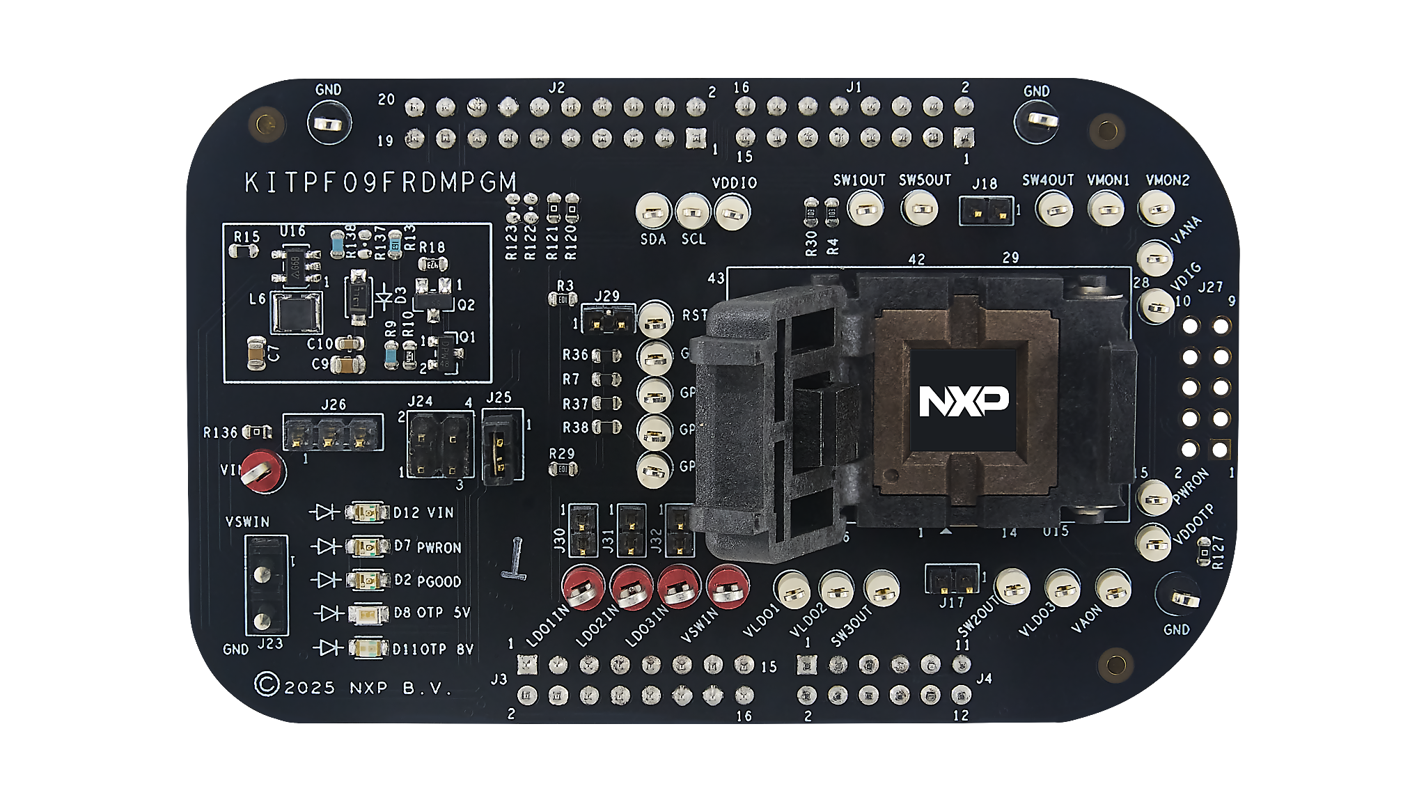
2 Get to Know the Hardware
The KITPF09FRDMPGM kit provides a platform for supporting designs based on the PF09 Family of NXP, not for evaluation. All PF09 Family features can be configured and programmed using NXP GUI software by accessing the registers in Read and Write mode. Output voltages, digital signals (I²C, RSTB, etc.) are accessible through hook connectors.
2.1 Board Features
- Header connectors for I/O configuration
- Selectable power input for programming
- Access pin connectors for accessing inputs and outputs
- Indicator LEDs green to indicate PGOOD, PWRON and VIN
- RED LED to indicate that the OTP 8 V burning voltage is set and BLUE LED to indicate that the OTP 5 V voltage is set
- Advanced system monitoring via the KL25Z MCU
- Embedded USB to I²C protocol for easy connection to the software GUI through the KL25Z MCU
2.2 Board Description
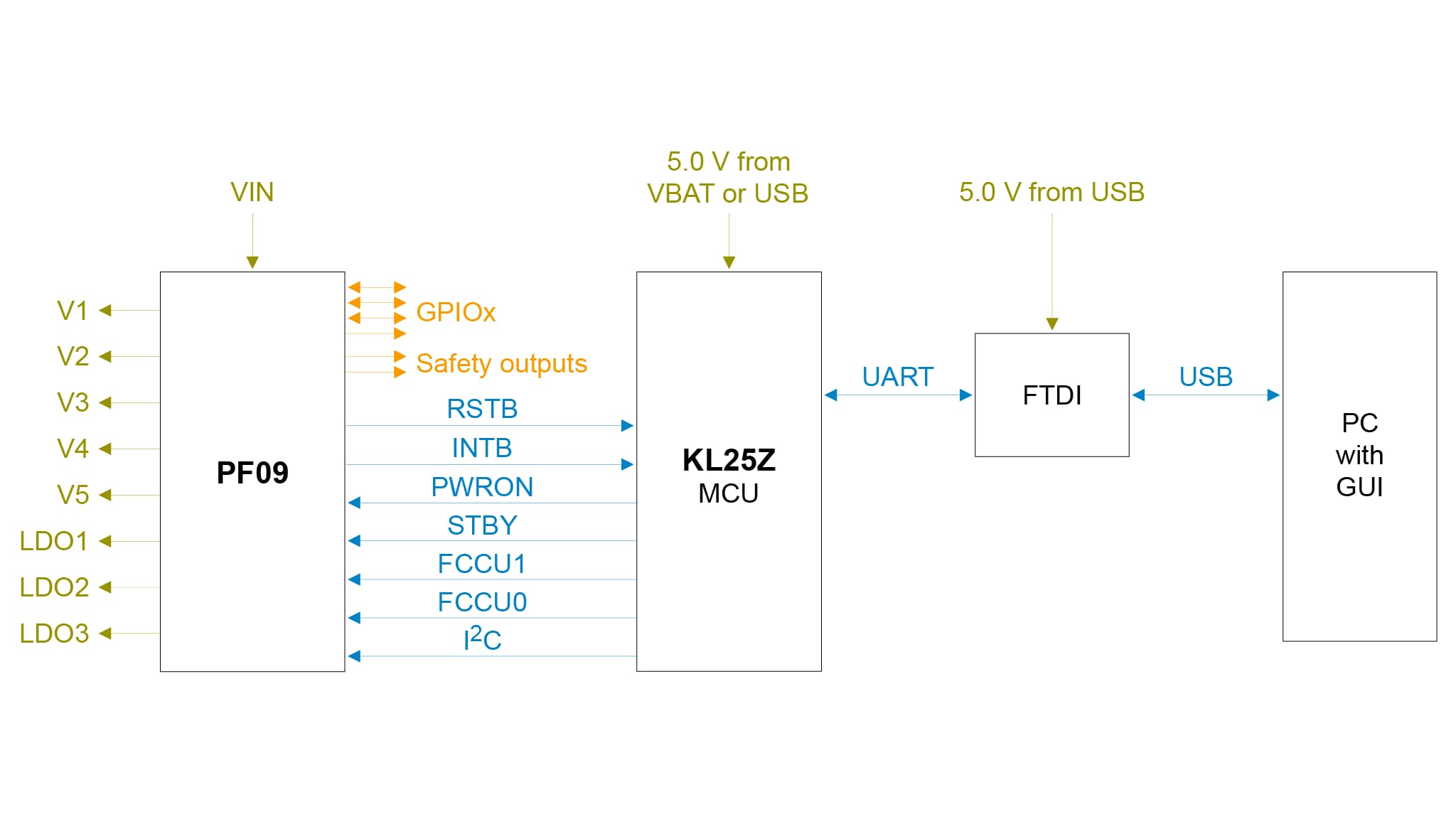
The hardware of the kit consists of the KITPF09FRDMPGM program board embedded with a KL25Z microcontroller, and the USB cable required to connect the board to the PC.
The KITPF09FRDMPGM program board features a socket that allows the user to fuse an individual PF09 Family using the device’s two time programmable (OTP) feature without extra tools. The board also contains LEDs and test points that provide a means of limited monitoring performance in real time. An emulation mode allows the user to test as many configurations as needed before programming the part.
The KL25Z is connected on the bottom side of the KITPF09FRDMPGM programming board. The role of the KL25Z is to manage I²C communication between the KITPF09FRDMPGM program board and the GUI installed on the PC. The KL25Z draws power either from the USB cable connected to the PC or from the battery supply (when not connected to the GUI).
3 Configure the Hardware
3.1 Configure the Hardware
The procedure for setting up the KITPF09FRDMPGM program board is as follows:
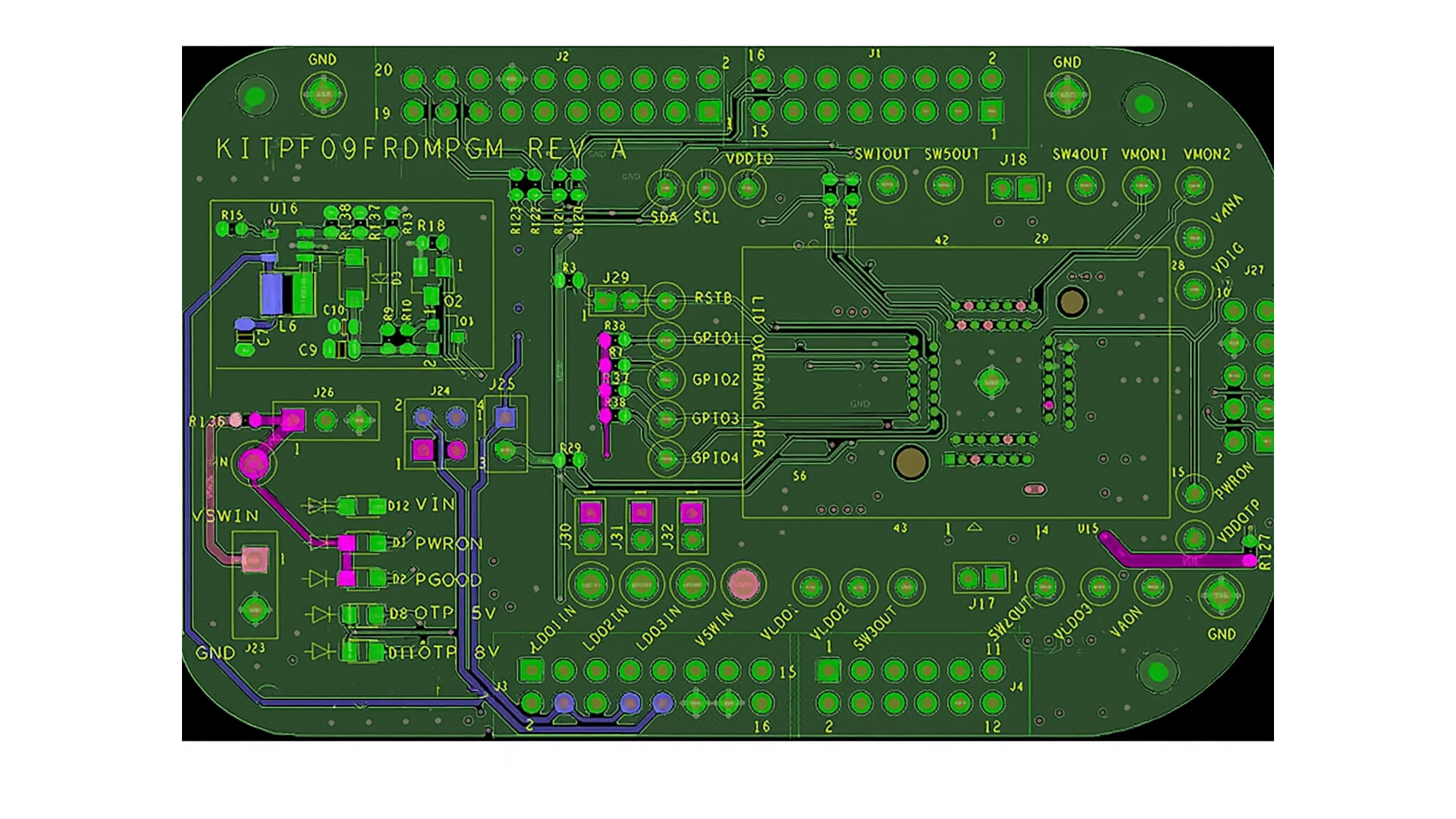
- Make sure that the board has the jumpers configured in their default positions. The default debug configuration enables the board to be fully controlled by the KL25Z MCU (via I²C) and the GUI. Section 3 shows the default jumpers configuration for the PF09 Family.
- Connect the power supply to VIN (hook connector). The power supply should be set to a nominal value of 5 V.
- Make sure the USB cable between the board and the PC is securely connected. This connection is critical because the USB port serves as a communication channel between the PC and the KL25Z MCU onboard, and also provides voltages and references to some onboard circuits.
This section describes the KITPF09FRDMPGM program board by explaining the features associated with each jumper and switch, giving information on hardware configuration to enable these features, and providing advice on LED signaling and test points available on the board.
The default debug configuration enables the board to be fully controlled by the KL25Z MCU (via I²C) and the GUI. Figure 2 shows the jumper location for PF09. See below for PF09 default jumpers configuration.
| Connector | Pin count | Line | Connection |
|---|---|---|---|
J1/J2/J3/J4 |
--- | FRDM board headers | --- |
J17 |
1 | SW2OUT |
Open |
| 2 | SW3OUT |
Open | |
J18 |
1 | SW4OUT |
Open |
| 2 | SW5OUT |
Open | |
J29 |
1 | Pullup for RSTB |
Jumper connected |
| 2 | RSTB |
||
J23 |
1 | VIN |
Open |
| 2 | GND |
Open | |
J24 |
1 | VIN |
Open |
| 2 | USB_PWR |
||
| 3 | VIN |
Open | |
| 4 | 3V3_MCU |
||
J25 |
1 | VDDIO |
Jumper connected |
| 2 | 3V3_MCU |
||
J26 |
1 | VIN |
Open |
| 2 | PWRON |
Open | |
| 3 | GND |
Open | |
J27 |
1 | SCL |
Open |
| 2 | PWRON |
Open | |
| 3 | SDA |
Open | |
| 4 | VDDOTP |
Open | |
| 5 | IO1 |
Open | |
| 6 | VDDIO |
Open | |
| 7 | R127 0Ohms to VIN |
Open | |
| 8 | GND |
Open | |
| 9 | Open | Open | |
| 10 | Open | Open |
| Function | Description | Color |
|---|---|---|
LDO1IN |
Monitoring point for the LDO1 input voltage |
Red |
LDO2IN |
Monitoring point for the LDO2 input voltage |
Red |
LDO3IN |
Monitoring point for the LDO3 input voltage |
Red |
VSWIN |
Switchers input voltage | Red |
VIN |
External Input voltage | Red |
VLDO1 |
Monitoring point for the LDO1 output |
White |
VLDO2 |
Monitoring point for the LDO2 output |
White |
VLDO3 |
Monitoring point for the LDO3 output |
White |
GND |
Board grounds direct connection -4 easy access points | White |
VAON |
Monitoring point for the VAON output |
White |
SW1 Output |
Monitoring point for the SW1 output |
White |
SW2 Output |
Monitoring point for the SW2 output |
White |
SW3 Output |
Monitoring point for the SW3 output |
White |
SW4 Output |
Monitoring point for the SW4 output |
White |
SW5 Output |
Monitoring point for the SW5 output |
White |
GPIO1 |
GPIO1 access point – bidirectional pin |
White |
GPIO2 |
GPIO2 access point – bidirectional pin |
White |
GPIO3 |
GPIO3 access point – bidirectional pin |
White |
GPIO4 |
GPIO4 access point – bidirectional pin |
White |
VMON1 |
Monitoring point for the external monitor VMON1 |
White |
VMON2 |
Monitoring point for the external monitor VMON2 |
White |
VDIG |
VDIG monitoring point |
White |
VANA |
VANA monitoring point |
White |
PWRON |
Power on input pin access point | White |
VDDIO |
VDDIO Monitoring point |
White |
RSTB |
System reset signal output monitoring point | White |
VDDOTP |
VDDOTP Monitoring point |
White |
I²C-SDA |
I²C SDA access point – bidirectional pin |
White |
I²C-SCL |
I²C SCL access point – bidirectional pin |
White |
Design Resources
Board Information
Additional References
In addition to our PF09: 9-Channel PMIC for High-Performance Applications, ASIL D and SIL 2 page, you may also want to visit: