Getting Started with the EVBMLC2HOST Evaluation Board
Contents of this document
-
Out of the Box
-
Get to Know the Hardware
-
Configure Hardware
Sign in to save your progress. Don't have an account? Create one.
Purchase your EVBMLC2HOST
1. Out of the Box
The NXP analog product development boards provide an easy-to-use platform for evaluating NXP products. The boards support a range of analog, mixed-signal and power solutions. They incorporate monolithic integrated circuits and system-in-package devices that use proven high-volume technology. NXP products offer longer battery life, a smaller form factor, reduced component counts, lower cost, and improved performance in powering state-of-the-art systems.
This page will guide you through the process of setting up and using the EVBMLC2HOST and EVBMLC2PER evaluation boards.
1.1 Kit Content and Packing List
The kit contents include:
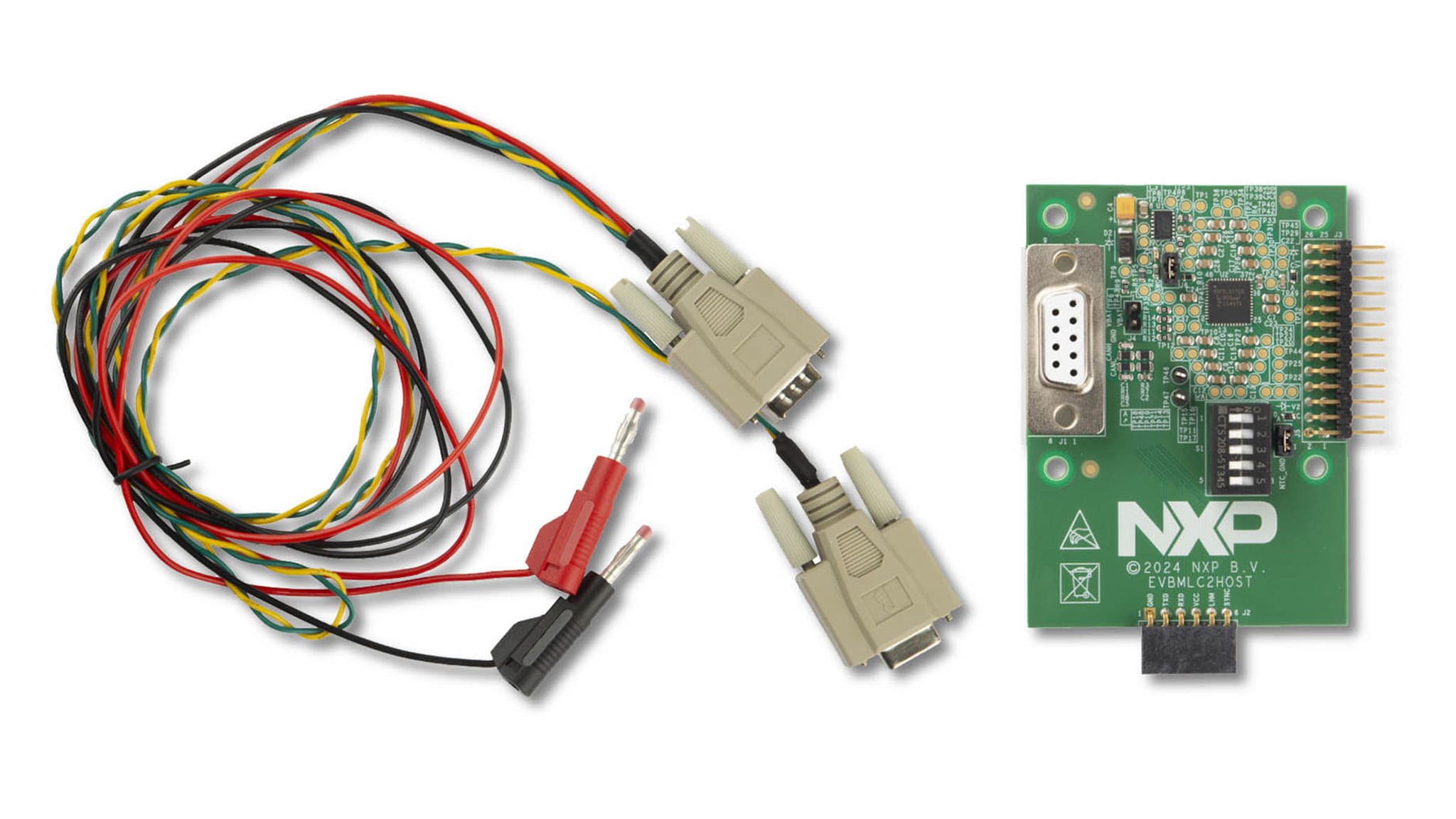
- Assembled and tested EVBMLC2HOST evaluation board in an antistatic bag. It includes an ASL6112SHN and an UJA1163ATK
- One cable consisting of a yellow/green twisted pair for CAN communication and a red/black cable pair for external power supply at 12 V. The yellow/green cable is terminated with male and female
D-Sub 9connectors. The red/black cable is terminated with banana jacks
1.2 Additional Hardware
In addition to the kit contents, the following hardware can be either beneficial or even necessary when working with the kit:
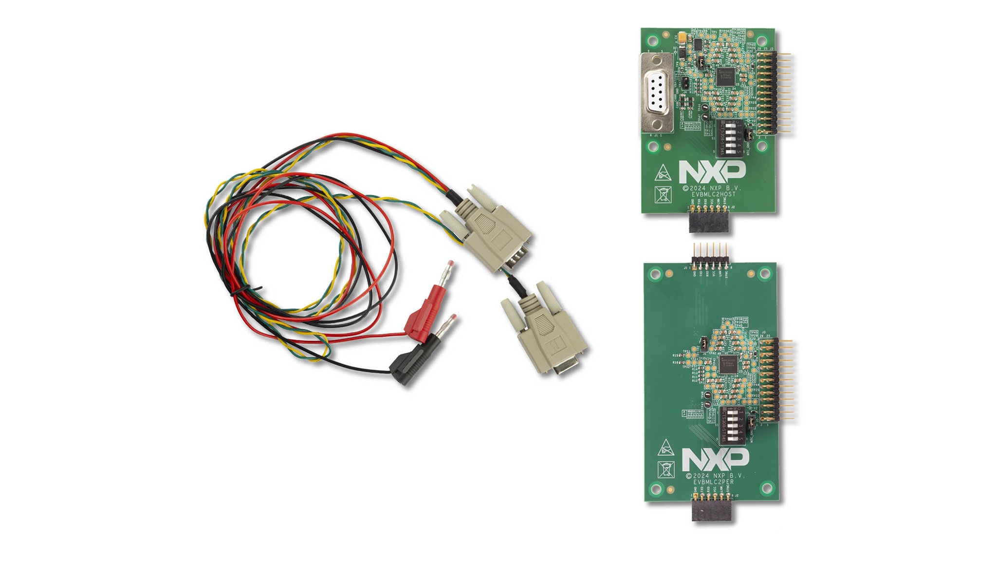
- EVBMLC2PER: The peripheral EVB that can be used to expand the capability of the host EVB, to
handle more LEDs
- This kit can be expanded by adding multiple peripheral EVBs
- If multiple peripherals are used, no external power is needed as the power supply comes via the connected host EVB or the adjacent peripheral EVB
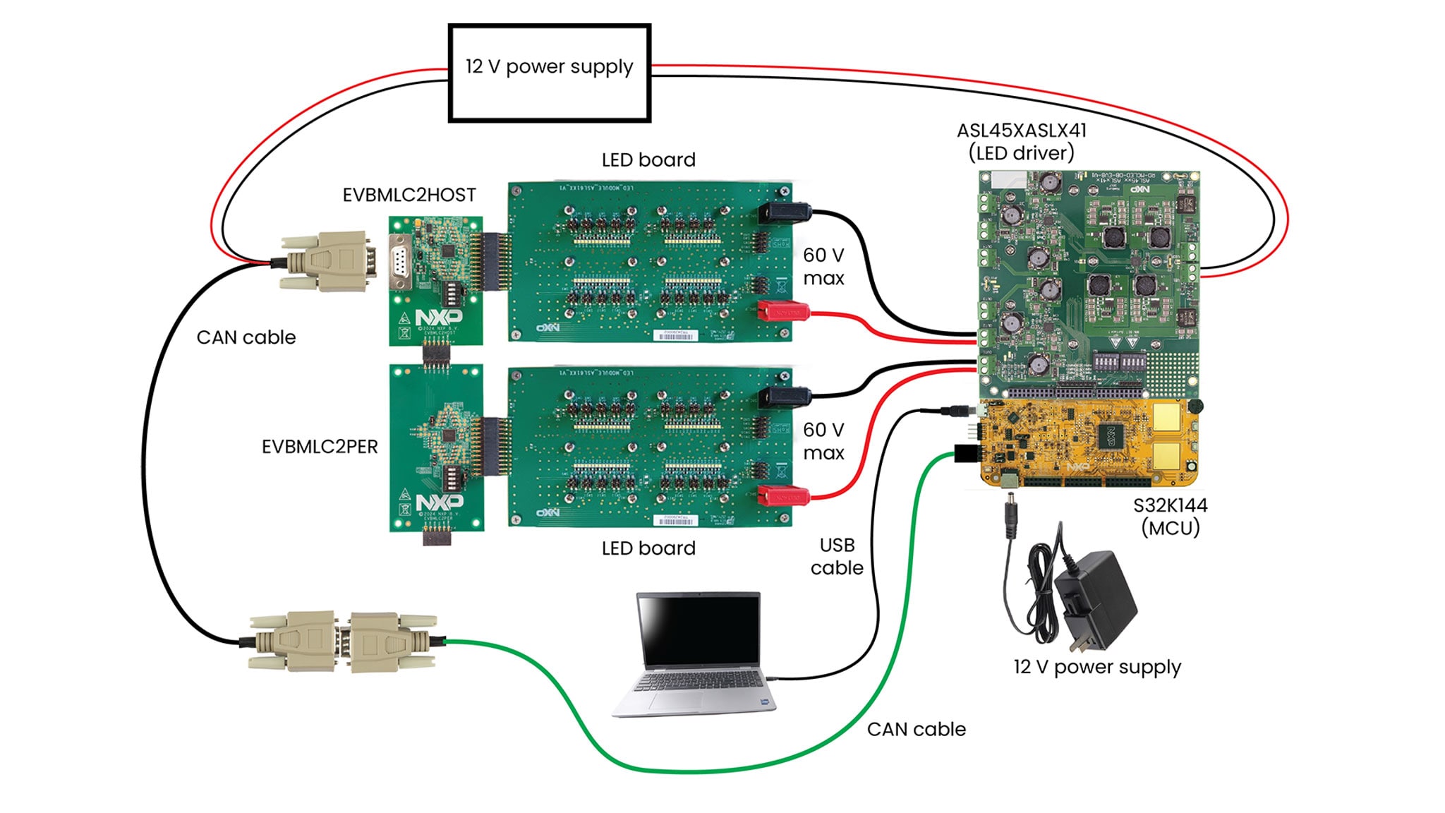
- LED board: Although an LED board is essential, the one shown in this manual is not for sale, as customers have their own LED configurations—normally different from each other—resulting from their own requirements
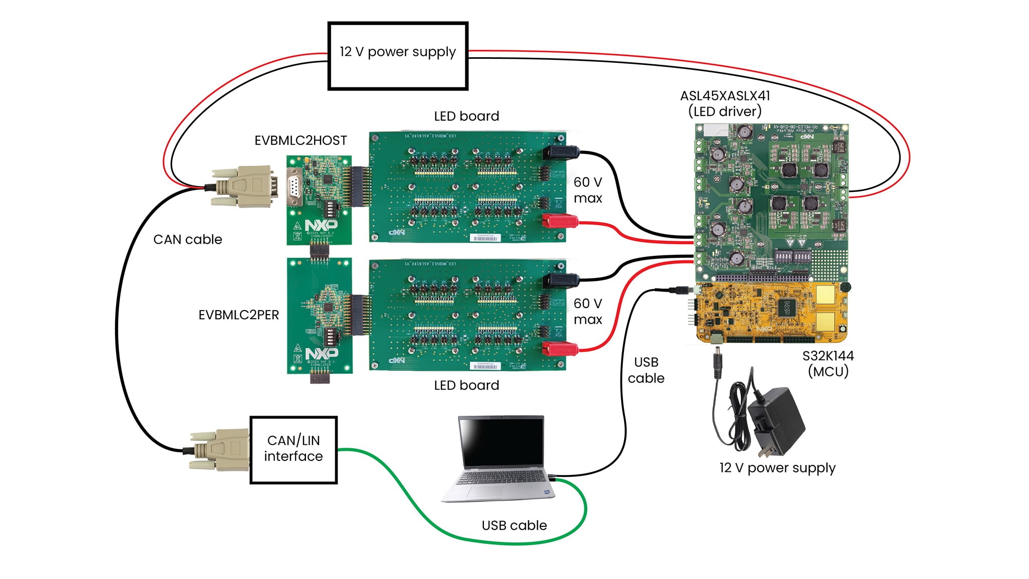
- ASL45XASLX41 evaluation board: It includes both the ASL4500SHN and ASL3416SHN integrated circuits (IC)
- S32K144 evaluation board: This board is highly recommended, and includes a microcontroller (MCU) for managing both EVBMLC2HOST and EVBMLC2PER via CAN interface and also manages the ASL45XASLX41
- Power supply: A single supply with multiple 12 V outputs or multiple 12 V supplies are necessary for EVBMLC2HOST, ASL45XASLX41 and S32K144 boards
- External CAN interface: This optional hardware can be, for example, a Vector VN1630A CAN/controller area network flexible data-rate (CAN FD) interface or similar, and is managed with the Vector CANoe software
The board is useful for individually powering up to six LED boards with a DC voltage of up to 60 V, while respecting a desired maximum current limit.
1.3 Minimum System Requirements
This evaluation board requires a laptop running Windows 10 or Windows 11 with at least one of these operating systems installed.
1.4 Software
Installing the software—NXP MLC GUI or, as an alternative, CANoe based GUI—is essential for being able to work with the evaluation kit.
- NXP machine learning core (MLC) graphical user interface (GUI):
- The required material and setup information are shown in Figure 3, and if using this option, no external CAN interface or CANoe software is needed
- The available firmware can be downloaded to the flash memory of the MCU mounted on the S32K144 evaluation board
- The graphical user interface (GUI) runs on a Microsoft-Windows-based laptop
- In addition to the software, in the download you find detailed documentation with installation instructions and a user manual
- MLC2 CANoe project:
- The required material and setup information are shown in Figure 4, depicting an option needing additional hardware—a Vector CAN interface—and the CANoe software
- Detailed usage instructions can be found in the ASL61XXYHZ_AN application note
2. Get to Know the Hardware
2.1 Board Features
The EVBMLC2HOST offers the possibility to modify the least significant part of the CAN address by positioning five switches. Furthermore, it integrates a 5 V low dropout regulator (LDO) and a CAN transceiver embedded in the UJA1163ATK system-basis chip (SBC).
Built into the ASL6112SHN, the EVBMLC2HOST additionally has the following features:
- 200 MHz oscillator
- 16 channels, arranged in four configurable blocks of four switches
- Flexible pulse width modulation (PWM) driver for the individual channel
- LED temperature measurement via negative temperature coefficient (NTC)
- Advanced diagnosis for LED open/short detection, nonfunctional switch detection, individual channel voltage measurement, and so on
- Synchronized frequencies when using multiple multi-level cell (MLC) devices
- Controller Area Network (CAN) communication logic
The EVBMLC2PER has the following features built into the ASL6112SHN:
- 200 MHz oscillator
- 16 channels, arranged in four configurable blocks of four switches
- Flexible PWM driver for the individual channel
- LED temperature measurement via NTC
- Advanced diagnosis for LED open/short detection, nonfunctional switch detection, individual channel voltage measurement, and so on
- Synchronized frequencies when using multiple MLC devices
- CAN communication logic
The EVBMLC2PER offers the possibility to modify the least significant part of the CAN address by positioning five switches.
However, as the EVBMLC2PER has no UJA1163ATK SBC, it misses the 5 V low dropout regulator (LDO) and the CAN transceiver. The reason being that for the EVBMLC2PER to work, it must be connected to the EVBMLC2HOST. The connection allows the EVBMLC2PER to access the 5 V low drop out (LDO) and the CAN transceiver present on the host board, which are shared hardware resources.
2.2 Board Description
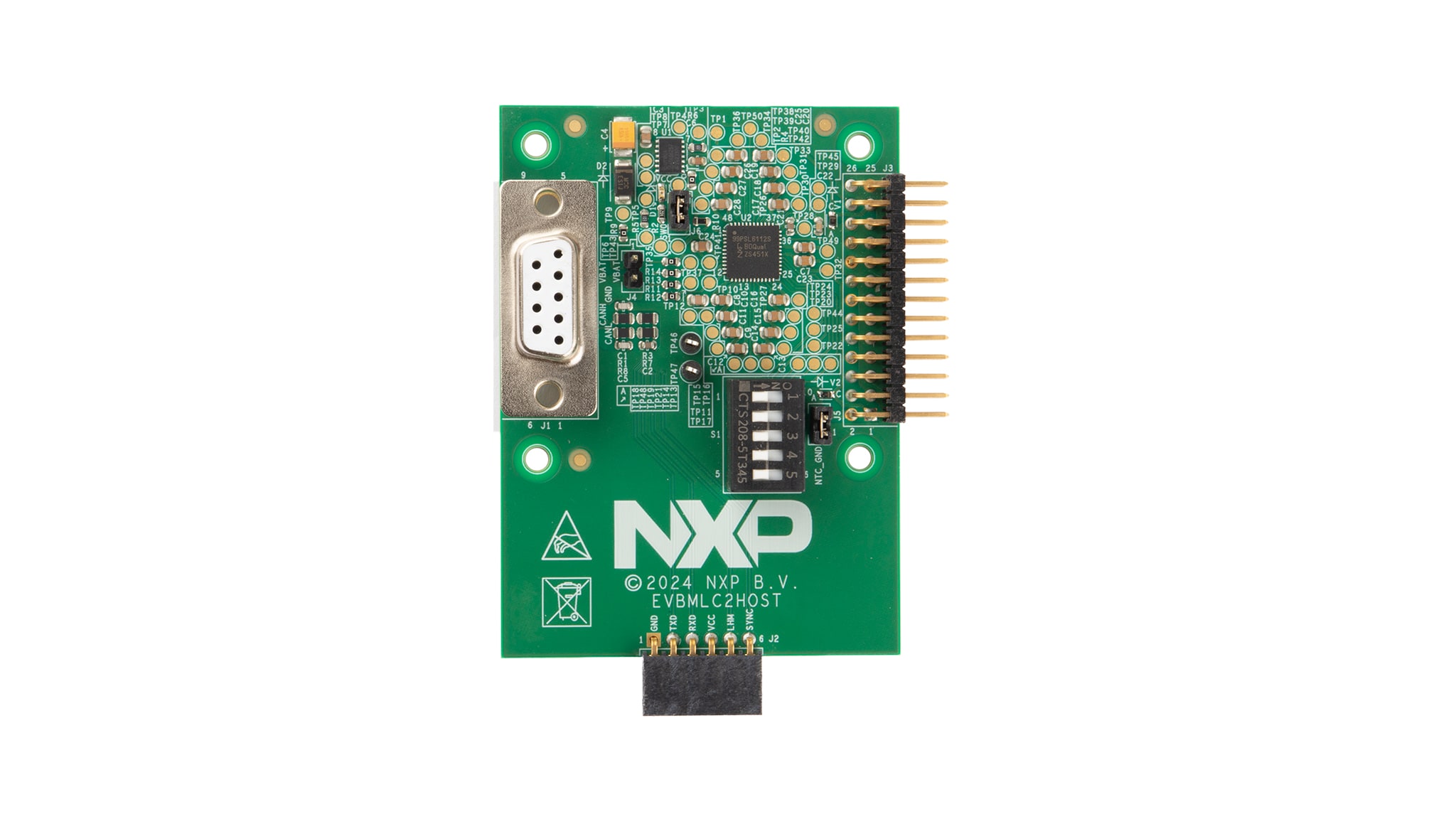
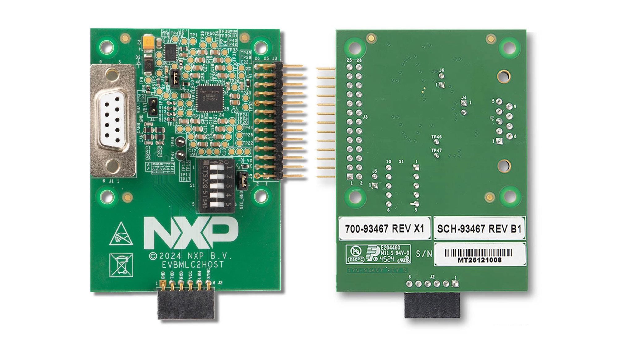
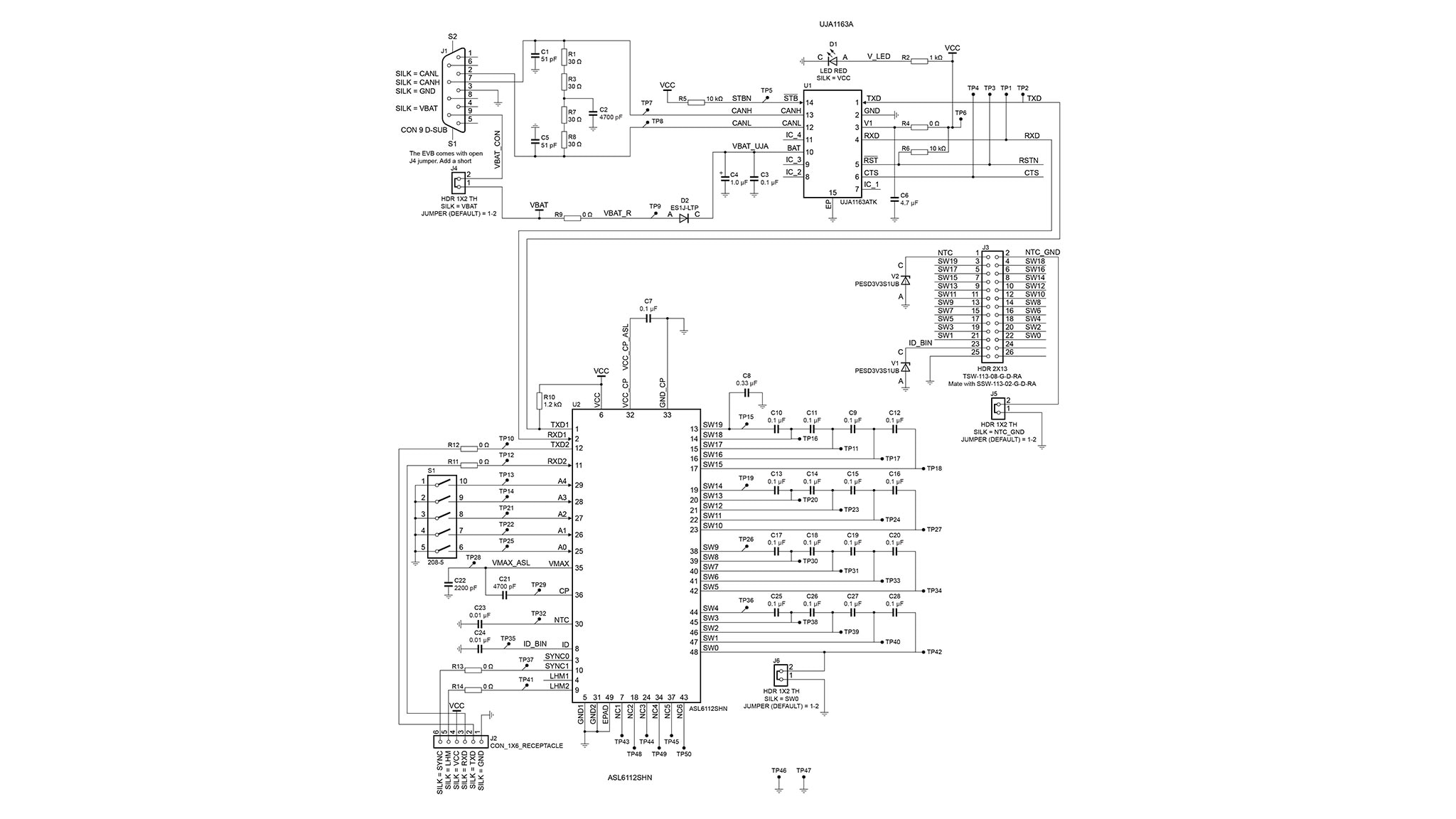
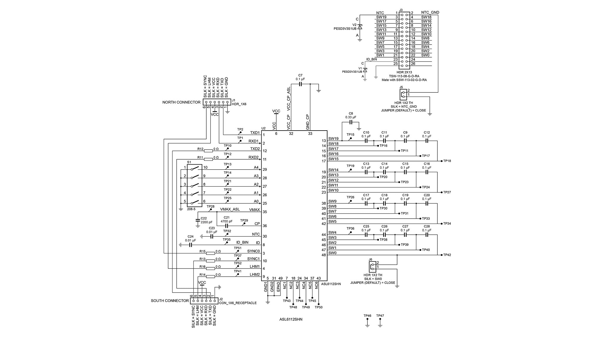
The EVBMLC2HOST, whose appearance is shown in Figure 5 and whose schematic is given in Figure 7, includes the following components:
- ASL6112SHN matrix LED controller
- UJA1163ATK SBC – Uses a 12 V input supply
J1femaleDB9sub-connector – Supplies the board with 12 V and communication via the CAN cableJ2female connector – Connects to EVBMLC2PER
(Plug the six-pin J1 male connector belonging to the EVBMLC2PER board into this connector)
J3male connector – Connects to LED boardJ4jumper – Controls supply to the board
(Add a short to this jumper, otherwise the board remains unsupplied, thus when the board is supplied, a red LED emits light)
- LED – Emits red light only if 12 V comes through the
DB9sub-connector and theJ4jumper has been provided with a short S1five-switch block – Sets the board physical address
The initial address is 0b11111 and is equivalent to decimal 32. The switch at position 5 corresponds to
the
least
significant bit, while position 1 corresponds to the most significant bit. It is highly recommended to change the
switch positions to get a small address. For instance, 0b00000 = 0 decimal. To get this address value,
move
all five switches shown in Figure 5 to the opposite position.
Notice that the ID resistor and the NTC have not been populated. This is because they belong to the domain of the LED board.
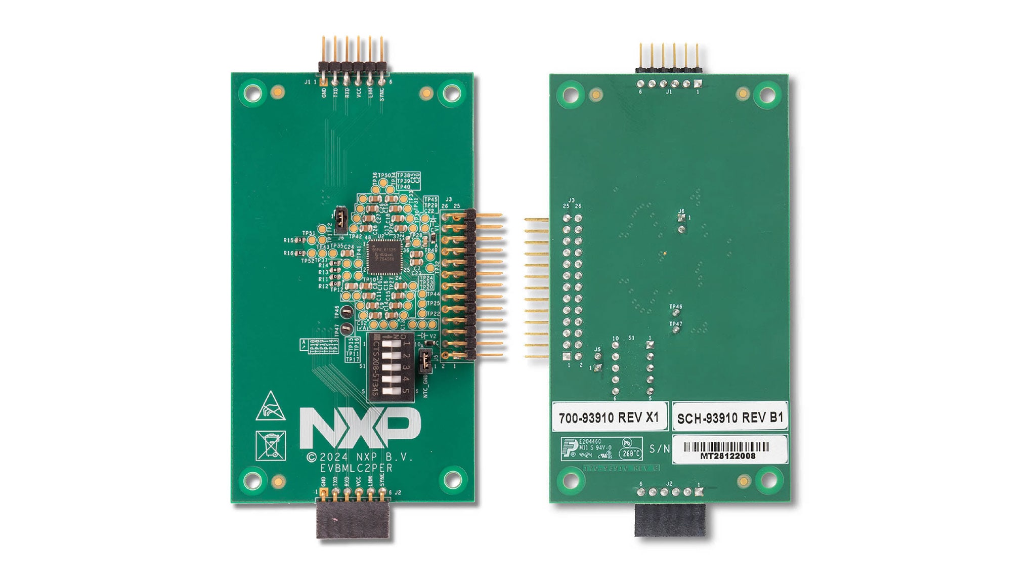
The EVBMLC2PER, whose appearance is shown in Figure 6 and whose schematic is given in Figure 8, includes the following components:
- ASL6112SHN matrix LED controller
J1male connector – Connects to EVBMLC2HOST
Plug the six-socket J2 female connector belonging to the EVBMLC2HOST board onto this connector.
J2female connector – Plugs onto the six pinsJ1male connector belonging to the adjacent boardJ3male connector – Connects to LED boardS1five-switch block – Sets the physical address of the ASL6112SHN
The initial address is 0b11111, equivalent to decimal 32. The switch at position 5 corresponds to the
least
significant bit, while position 1 corresponds to the most significant bit. It is highly recommended to change the
switch positions to get a small address (for instance 0b00001 = 1 decimal). To get this address value,
the four
switches labeled 1 to 4, shown in Figure 6, must be moved to the opposite position. For a peripheral board,
it is good practice to use a higher address than the host card address. If more peripherals needed, continue
incrementing the address by one unit.
Notice that the ID resistor and the NTC have not been populated. This is because they belong to the domain of the LED board.
3. Configure Hardware
3.1 Board Information
The schematics of the boards follow. For board layout and routing information, see reference 1 in Section 3.2.
3.2 Additional References
NXP Semiconductors provides online resources for this evaluation board and its supported devices on NXP.
- EVBMLC2HOST (KIT-ASL6112SHN) product
- NXP MLC GUI (the software you must be able to work with the kit): Once in the page, look for the GUI App for Matrix LED Controller (MLC)
- EVBMLC2PER (an optional EVB you can buy to expand the kit)
An alternative evaluation GUI—usable under the CANoe environment—can be downloaded by logging in to your secured NXP account. Once in the secured area, type the following string in the search bar: "ASL6112SHN CANoe project". You will be redirected to the download. The Vector CANoe project is intended for those who have a Vector CAN interface, such as the VN1630A.
Design Resources
Board Documents
Additional References
In addition to our ASL61XXYHZ, you may also want to visit: Automotive Advanced Exterior Lighting.