FS86 Automotive Kit Guides
Contents of this document
-
Out of the Box
-
Get Hardware
-
Get Software
-
Configure Hardware
Sign in to save your progress. Don't have an account? Create one.
Purchase your KITFS86AUTFRDMEM | FS86 Safety SBC Evaluation Board
1. Out of the Box
The NXP analog product development boards provide an easy-to-use platform for evaluating NXP products. The boards support a range of analog, mixed-signal and power solutions. They incorporate monolithic integrated circuits and system-in-package devices that use proven high-volume technology. NXP products offer longer battery life, a smaller form factor, reduced component counts, lower cost, and improved performance in powering state-of-the-art systems.
This page will guide you through the process of setting up and using the KITFS86AUTFRDMEM board.
1.1 Kit Contents and Packing List
The KITFS86AUTFRDMEM contents include:
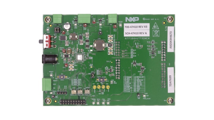
- Assembled and tested KITFS86AUTFRDMEM connected to a FRDM-KL25Z in an antistatic bag
- Jumpers mounted on board
- 3.0 ft USB-STD A to USB-B-mini cable
- Two connectors, terminal block plug, 2 pos., str. 3.81 mm
- Two connectors, terminal block plug, 3 pos., str. 3.81 mm
- Quick Start Guide
1.2 Additional Hardware
In addition to the kit contents, the following hardware is necessary or beneficial when working with this kit.
- Power supply with a range of 8.0 V to 40 V and a current limit set initially to 1.0 A (maximum current consumption can be up to 6.0 A)
1.3 Windows PC Workstation
This reference design requires a Windows PC workstation. Meeting these minimum specifications should produce great results when working with this evaluation board.
- USB-enabled computer with Windows 7 or Windows 10
1.4 Software
Installing software is necessary to work with this evaluation board. All listed software is available on the evaluation board's information page at KITFS86AUTFRDMEM or from the provided link.
- NXP GUI for automotive PMIC families - latest version
2. Get Hardware
2.1 Board Features
- VBAT power supply connectors (Jack and Phoenix)
- VPRE from 3.3 V to 5.0 V with output capability up to 10 A
- VBUCK from 1.0 V to 3.3 V
- VBOOST from 5.0 V to 6.0 V
- LDO1 from 1.5 V to 5.0 V
- LDO2 from 1.1 V to 5.0 V
- Ignition key switch
- FS0B external safety pin
- FRDM-KL25Z with embedded USB connection to NXP GUI for register access, OTP emulation and programming (access to I2C-bus, IOs, debug, AMUX and regulators)
- LEDs that indicate signals and regulator status
- Support OTP fuse capabilities
2.2 Board Description
The KITFS86AUTFRDMEM is a hardware evaluation tool that allows performance test. The FS8600 family can be evaluated with this board because it is populated with a superset part. The PFS8613xMDA0ES part soldered on the board can be fused twice.
An external LDO provides SUP_I²C voltage with a choice of 1.8 V or 3.3 V (default). SUP_I²C is intended to power FS86 I²C communication. From USB voltage, an external DC-DC generates the OTP programming voltage (8.0 V) without any need for an external power supply.
2.3 Board Components
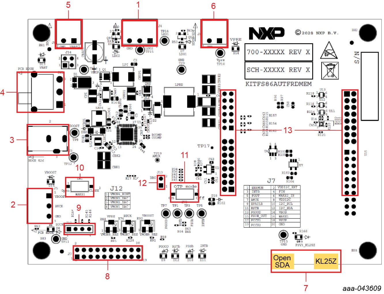
| Number | Description |
|---|---|
| 1 | LDO1 / LDO2 power supply |
| 2 | BUCK / BOOST power supply |
| 3 | VBAT Jack connector |
| 4 |
VBAT three position switch
|
| 5 | VBAT Phoenix connector |
| 6 | VPRE power supply |
| 7 | USB connectors (Open SDA for MCU flash; KL25Z for NXP GUI control) |
| 8 | Debug connectivity. Access to FS8600 signals |
| 9 | External regulator connectors (to VMONx) |
| 10 | WAKE1 switch |
| 11 | OTP mode switch |
| 12 | DBG pin to 0 V if unplugged |
| 13 | KL25Z FRDM board connectors |
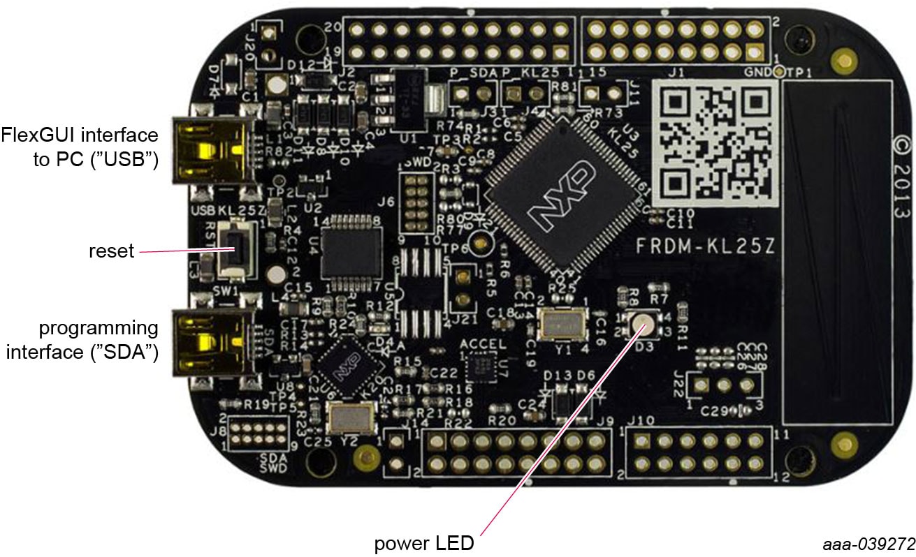
Kinetis KL25Z FRDM Board
The FRDM KL25Z is an ultra low-cost development platform for Kinetis L series MCU built on Arm Cortex-M0+ processor.
3. Get Software
3.1 Install Software
The device configuration can be programmed twice and emulated indefinitely using the GUI.
Device programming and emulation steps are described in the NXP GUI for FS86 Automotive Family User Manual available at NXP GUI for Automotive PMIC Families.
4. Configure Hardware
4.1 Configure the Hardware
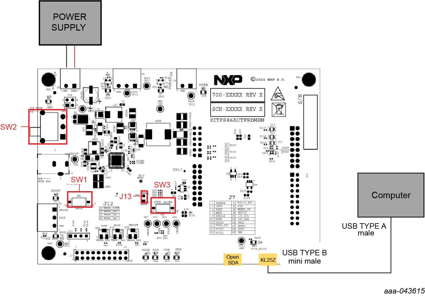
To configure the hardware, complete the following procedure:
-
Install jumpers and switches for the configuration shown in
Table 2
Switch Configuration Normal mode Debug mode entry OTP mode entry Operation watchdog 2s window watchdog window fully open OTP emulation / programming and Debug mode entry J13(DBG)open connect 1 to 2 DBG pin voltage pulled to 4.5 V or 8.0 V (SW3) SW1 (WAKE1) close (WAKE1 high) SW2 (VBAT) middle position (VBAT OFF) SW3 (DBG_OTP) open (DBG = 4.5 V) close (OTP mode ON) - Connect the Windows PC USB port to the KITFS86AUTFRDMEM development board using the provided USB 2.0 cable
-
Set the DC power supply to 12 V and current limit to 1.0 A.
With power turned off, attach the DC power supply positive and
negative output to KITFS86AUTFRDMEM VBAT Phoenix
connector (
J6) - Turn on the power supply
- Put SW2 in TOP position
At this step, if the product is in OTP mode entry configuration, all regulators are off. The user can then power-up with OTP configuration or configure the mirror registers before powering up. Power-up is effective as soon as one of the following action occurs:
J13jumper is removed- SW3 is switched off
- OTP mode exit command is sent by I²C
- NXP GUI button "Exit OTP Mode" is clicked
Design Resources
Board Documents
Additional References
In addition to our FS86: Safety System Basis Chip For Domain Controller, Fit For ASIL B and D page, you may also want to visit:
- FS8500: Safety System Basis Chip for S32 Microcontrollers, Fit for ASIL D
- FS8400: Safety System Basis Chip for S32 Microcontrollers, Fit for ASIL B
- NXP GUI for Automotive PMIC Families
Application pages: V2X Communications