Getting Started with the LID2580-NCJ29D6 Evaluation Board
Contents of this document
-
Out of the Box
-
Get Hardware
-
Install Software
-
Configure Hardware
Sign in to save your progress. Don't have an account? Create one.
Purchase your LID2580
1. Out of the Box
The NXP analog product development boards provide an easy-to-use platform for evaluating NXP products. The boards support a range of analog, mixed-signal and power solutions. They incorporate monolithic integrated circuits and system-in-package devices that use proven high-volume technology. NXP products offer longer battery life, a smaller form factor, reduced component counts, lower cost and improved performance in powering state-of-the-art systems.
This page will guide you through the process of setting up and using the LID2580-NCJ29D6 Evaluation Board.
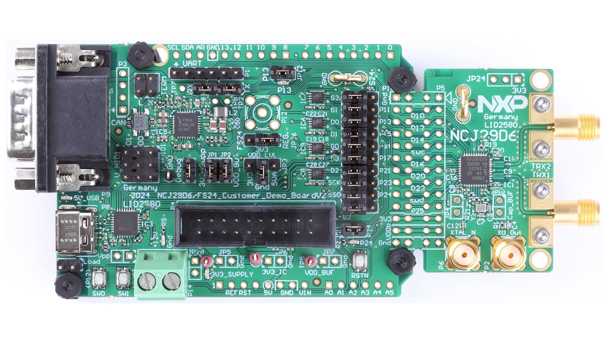
1.1 Kit Contents and Packing List
The kit contents include:
- Assembled and tested the evaluation board in an antistatic bag
- Quick Start Guide
- The NCJ29D6, which is a UWB device, capable of performing UWB-based ranging and radar
- An integrated CAN transceiver, switch mode regulator, watchdog circuit and other features
The FS24 is a CAN system basis chip, which offers:
1.2 Software
Installing software is necessary to work with this evaluation board. All listed software is available on the evaluation board's information page at the LID2580 Evaluation Board or from the provided link.
- For more details regarding the configurability of the bridge IC and where to download the necessary configuration software, refer to the FT4222H documentation of FTDI chip found at the FTDIChip page.
2. Get Hardware
2.1 Board Features
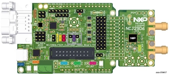
The demo board consists of two logical parts:
- The shield board contains all peripheral devices, including the FS24 SBC
- The UWB reference design contains the UWB IC and all necessary components for it to operate
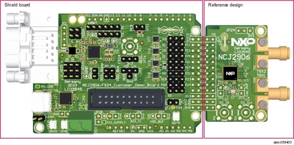
The shield board holds all components and connectors that are required to connect the reference design to a car, a larger demo system or a debugger. It holds:
- CAN connectors (Sub-D9 and pinheader)
- UART connector
- SWD connector for flashing and debugging
- Linear voltage regulator
- FS24 system basis chip and its peripherals
- USB connector for data communication and power supply
- Various test points and jumpers for different measurements and configurations
- LEDs and pushbuttons
- Arduino-compatible header that connects the board to a microprocessor board
The reference design holds the NCJ29D6 and the high-frequency part. If a good RF performance is to be achieved, these parts of the design are the most challenging. Therefore, the reference design is designed so that customers can cut it from the shield board and connect it to an individually designed prototyping board. This method reduces the hardware design effort at the beginning of a project. The following elements are present in the reference design:
- NCJ29D6 UWB IC
- XTAL with clock_in and clock_out option
- Landing patterns for buffer capacitors
- Two SMA connectors to attach external antennas
- Breakout connector to reconnect the reference design after separating it from the shield board. It can also be used to connect to an individually designed board or to interact with the pins of NCJ29D6 directly
3. Install Software
3.1 Install Software
The demo board is designed to operate in two different communication modes. It can either run as a USB device connected to a PC or as a device within a CAN bus network. To evaluate the NCJ29D6, NXP suggests using the USB device mode with some on-host software available via NXP.
4. Configure Hardware
4.1 Configure the Hardware
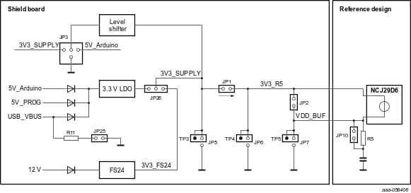
The jumpers have the following functions:
-
JP1: The complete UWB IC current runs through the jumperJP1. Connecting a current probe between the jumper pins allows the measurement of the IC current. See the arrow for the direction of the current flow -
JP2: Bypass of the NCJ29D6 internal current limiter. In the default configuration, this jumper must be closed -
JP3: Selection of the reference voltage of the level translators. -
JP5: Do not close that jumper. It is used to measure the voltage of the 3.3 V power domain. An external voltage supply to the UWB IC can also be connected here. The pin close to the edge of the PCB is connected to the ground -
JP6: Do not close that jumper. It is used to measure the supply voltage of the UWB IC. The pin close to the edge of the PCB is connected to the ground -
JP7: Do not close that jumper. It is used to measure the voltage of the buffer capacitor. The pin close to the edge of the PCB is connected to the ground -
JP10: This jumper is used to connect the buffer capacitor bank to the UWB IC. Typically, this jumper is closed. Remove theJP10jumper to enable the current limiter of NCJ29D^ only in keyfob operation -
JP25: This jumper connects a load resistor to the USB supply pins. It increases the permanent current consumption of the USB connector. If the board is powered via a USB power bank, this extra current prevents the power bank to enter shutdown mode and disabling its power output -
JP26: It is used to select either the LDO or the FS24 to supply the 3.3 V domain of the board.
Design Resources
Board Information
Additional References
In addition to NCJ29D6: Secure UWB IC for Automotive Ranging and Radar Applications you may also want to visit: