Getting Started with the MR-BMS771
Contents of this document
-
Out of the Box
-
Get Hardware
-
Configure Hardware
Sign in to save your progress. Don't have an account? Create one.
Purchase your MR-BMS771
1. Out of the Box
The NXP analog product development boards provide an easy-to-use platform for evaluating NXP products. The boards support a range of analog, mixed-signal and power solutions. This incorporates monolithic integrated circuits and system-in-package devices that use proven high-volume technology. NXP products offer longer battery life, a smaller form factor, reduced component count, lower cost and improved performance in powering state-of-the-art systems.
This page guides you through the process of setting up and using the MR-BMS771 board.
1.1 Kit Contents
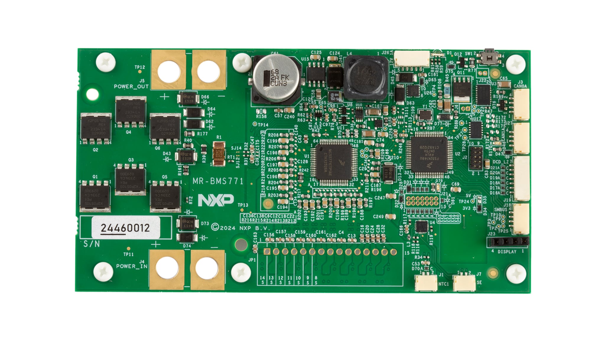
- Assembled and tested MR-BMS771 in an antistatic bag
- Controller Area Network (CAN) bus termination resistor (DRONE-CAN-TERM)
- Unmounted cell connectors for 8S to 14S with pre-crimped wires
- 4-pin Japan Solderless Terminal (JST)-GH to 4-pin JST-GH 300 mm cable (CAN)
- Power input and power output connectors
- External thermistor with cable
- Small SSD1306 Organic Light-Emitting Diode (OLED) display
- Quick start guide
- Small cell count selector interposer boards (7-cell to 14-cell)
- An Near Field Communication (NFC) antenna
1.2 Additional Hardware
In addition to the kit contents, the following hardware is necessary or beneficial when working with this kit.
- Battery pack (7S to 14S with cell balancing connector) with a range of 15 V to 59 V and a current limit of 30 A DC (up to 30 A DC has been tested)
- Suitable charger for the battery
- Soldering iron to configure the board
- PEmicro Multilink Universal or SEGGER J-Link Mini debugger or other suitable debugger
- Optional The DCD-LZ adapter
1.3 Software
Installing software is necessary to work with this reference design. All listed software is available on the reference design information page at MR-BMS771.
- S32 Design Studio (DS) for Arm®-based MCUs (recommended)
- Model-Based Design Toolbox (MBDT) example (recommended)
- NuttX Real-Time Operating System (RTOS) C-based BMS example application
2. Get Hardware
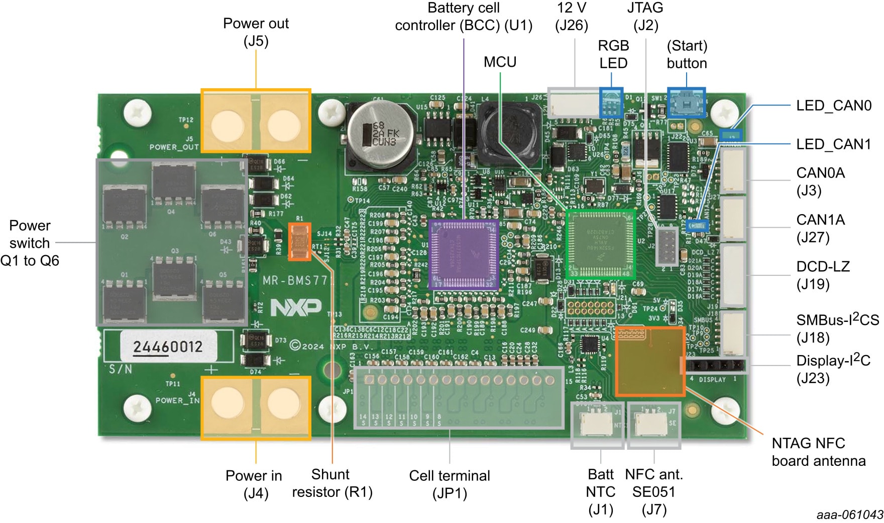
2.1 Board Features
- Supports battery from 7S to 14S, with stack voltage ranging from 15 V to 59 V
- Measures battery stack and cell voltages, and battery charge or discharge current up to 30 A DC tested
- Passive cell-balancing option over ~66 Ω balance resistors per cell
- Offers a deep-sleep mode (for transportation and storage) with low leakage current, and an automatic-sleep mode with low current consumption on the battery
- Allows CAN, Inter-Integrated Circuit (I²C) and NFC communication
- Implements Serial Wire Debug (SWD) and Joint Test Action Group (JTAG) debugging interfaces, and works with standard J-Link and other debuggers
- Implements DCD-LZ combined debug console interface for use with PX4 Dronecode and HoverGames platforms
2.2 Board Description
The MR-BMS771 is a standalone BMS reference design suitable for mobile robotics, such as drones and rovers that supports 7-cell to 14-cell batteries.
The device performs analog-to-digital conversion on the differential cell voltages and currents. It is capable of accurate battery charge coulomb counting and battery temperature measurements. It can also communicate with a flight management unit (FMU) through DroneCAN/CyphalCAN and/or a System Management Bus (SMBus).
3. Configure Hardware
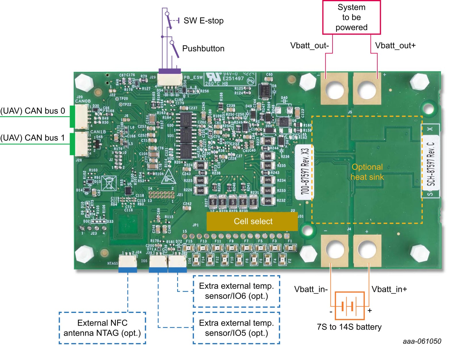
3.1 Power Connectors
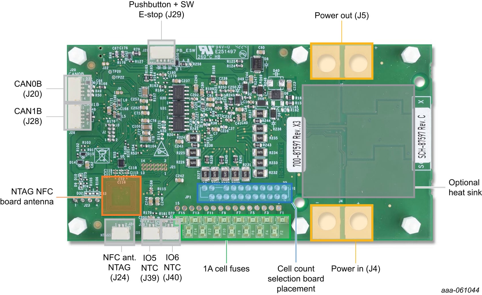
As the MR-BMS771 board aims to be adaptable for every battery setup, power and battery cell-terminal connectors are not pre-mounted on the Printed Circuit Board (PCB). This allows the user to configure the board with the connector.
The power-connector footprints on the design correspond to the DFRobot FIT0588 connector. These footprints also support soldering typical insulated heavy-gauge power wires. TE Connectivity provides a line unmanned power (UMP) connectors, specifically for professional high‑power mobile systems.
3.2 Cell Terminal Connection
The MR-BMS771 board can be configured to fit 7S to 14S battery packs.
Depending on the desired configuration, some adjustments must be made on the board:
- The correct cell-terminal connector must be soldered as Jumper Position 1 (JP1) on the top side (7S to 14S connectors are provided in the kit).
- By soldering the correct small cell-count selector interposer board, the connection to the cell terminal circuit is done.
3.3 Shunt Resistor
The shunt resistor (R1) can be disconnected from the overcurrent protection circuit and the Battery Control Circuit (BCC) by opening the
SJ13 and SJ14 jumpers. Both jumpers are closed by default.
3.4 External NFC Antenna
The external antenna is selected by default.
The onboard NTAG 5 chip is designed to provide active antenna matching and amplification, giving enhanced performance when the battery is present and providing power. However, for extended-range operation, an external NFC antenna can replace the PCB antenna.
To use the PCB antenna, the user must reconfigure the board using the following steps:
- Place both 0.75 Ω resistors R93 and R94
- Replace capacitor C72 (56 pF) with an 82 pF capacitor and capacitor C116 (680 pF)
The NTAG 5 chip is not installed for the first batch.
3.5 Optional Components
Heat sink
Depending on the application, the user can add an optional heat sink onto the MR-BMS771 board. The recommended part to use as a heat sink is the HSB30-373710.
It is recommended that you use an electrically isolated yet quality thermally conducive layer (for example, a special adhesive tape) between the BMS771 and the heat sink. This will improves the thermal conductivity.
Design Resources
Board Information
Additional References
In addition to our MR-BMS771 page, you may also want to visit:
- MC33771C 14-Channel Li-Ion Battery Cell Controller IC
- UJA1169ATK Mini High-Speed CAN System Basis Chip
- S32K S32K Automotive General-Purpose Microcontrollers
- NTAG5-BOOST NFC Forum-Compliant I²C Bridge for Tiny Devices
- TJA1463 CAN Signal Improvement Capability Transceiver with Sleep Mode
- SE051 Proven, Easy-to-Use IoT Security Solution with Support for Updatability and Custom Applets