Getting started with the PCA9422 Evaluation Board User Manual
Contents of this document
-
Out of the Box
-
Get to Know the Hardware
-
Configure Hardware
Sign in to save your progress. Don't have an account? Create one.
Purchase your PCA9422-EVB
1. Out of the Box
The NXP analog product development boards provide an easy-to-use platform for evaluating NXP products. The boards support a range of analog, mixed-signal and power solutions. They incorporate monolithic integrated circuits and system-in-package devices that use proven high-volume technology. NXP products offer longer battery life, a smaller form factor, reduced component counts, lower cost and improved performance in powering state-of-the-art systems.
This page will guide you through the process of setting up and using the PCA9422 board.
1.1 Kit Content and Packing List
The kit content includes:
- Assembled and tested PCA9422-EVB evaluation board in an antistatic bag
-
Available evaluation board revisions:
- SCH Rev F1 includes the PCA9422B PMIC version, operating all buck regulators at 4 MHz.
- SCH Rev F2 includes the PCA9422M PMIC version, operating all buck regulators at 2 MHz.
- USB-C Cable
- Spare jumpers
1.2 Additional Hardware
In addition to the kit contents, the following hardware is necessary or beneficial when working with this board.
- 1-cell Li-ion battery
- 5.0 V power supply or USB with enough current capability (VIN requires 1.2 A or above and VBAT requires 3.2 A or above for maximum power output)
- PCA9422 GUI installed on a Windows PC
- Multimeters to measure regulator outputs or other voltages
- Oscilloscope (optional)
- USB enabled computer running Windows 7, 8, or 10
1.3 Software
The PCA9422 GUI is available on the evaluation board's information page at PCA9422 or from the provided link in the Design Resources section of this guide. Please ensure that the PCA9422 GUI is installed on a Windows PC.
2. Get to Know the Hardware
The PCA9422 is a highly integrated power management IC (PMIC), targeted to provide a full power management solution for low power microcontroller applications or other similar applications.
2.1 Board Features
The device consists of a linear battery charger capable of charging up to 640 mA current. It has an I²C programmable constant current (CC) and constant voltage (CV) values for flexible configuration. Various built-in protection features such as input overvoltage protection, overcurrent protection, thermal protection, etc. are also provided for safe battery charging. It also features JEITA compliant charging.
The device also integrates three step-down DC/DC converters (bucks) which have I²C programmable output voltage. All buck regulators have integrated high-side and low-side switches and related control circuitry, to minimize the external component counts, a pulse-frequency modulation (PFM) approach is utilized to achieve better efficiency under light load condition. Other protection features such as overcurrent protection, undervoltage lockout (UVLO), and so on, are also provided. By default, the input for these regulators is powered from either VIN or VBAT, whichever is greater.
One ultralow quiescent Buck-Boost converter is designed to power system peripherals that require voltages higher and/or lower than the battery voltage, it seamlessly transitions between buck, buck-boost and boost modes, minimizing discontinuities and subharmonics in the output voltage ripple.
In addition, four on-chip LDO regulators are provided to power up various voltage rails in the system. One LDO is for SNVS core power supply, two 200 mA NMOS LDOs with load switch feature are capable of regulating to low output voltage from buck regulator output. One 200 mA PMOS LDO is intended to supply power to microcontroller or peripheral devices. Other features such as FM+ I²C-bus interface, device enable, interrupt signal, etc. are also provided.
The chip is offered in a 2.90 mm x 3.00 mm, 7 x 7 bump, 0.4 mm pitch WLCSP package.
- Linear battery charger for charging single cell Li-ion battery
- 26 V tolerance on VIN pin
- Programmable input OVP (5.5 V)
- Programmable constant current (up to 640 mA) and precharge low voltage current threshold
- Programmable constant voltage regulation
- Programmable automatic recharge voltage and termination current threshold
- Built-in protection features such as input over voltage protection (OVP), battery over current protection (OCP), thermal protection
- JEITA compliant
- Battery attached detection
- Overtemperature protection
- Three step-down DC/DC converters
- Very low quiescent current
- Programmable output voltage
- SW1: core buck converter, 0.4 V~1.975 V output, 6.25 mV/step, up to 500 mA
- SW2: system buck converter, 0.4 V~3.4 V output, 25 mV/step, up to 500 mA
- SW3: core buck converter, 0.4 V~1.975 V output, 6.25 mV/step, up to 500 mA
- Low power mode for extra powersaving
- One Buck-Boost converter
- Ultralow quiescent current
- High-efficient Boost mode
- Seamlessly transition between Buck, Boost and Buck-Boost modes
- 2.5 V~5.5 V input and 1.8 V~5.0 V output, 25 mV/step, up to 500 mA
- Four LDOs
- Programmable output voltage regulation
- LDO1: always-on LDO, 0.8 V~3.0 V output, 25 mV/step, up to 10 mA
- LDO2: system LDO/Load switch, 0.5 V~1.95 V output, 25 mV/step, up to 200 mA
- LDO3: system LDO/Load switch, 0.5 V~1.95 V output, 25 mV/step, up to 200 mA
- LDO4: LDO, 0.8 V~3.3 V output, 25 mV/step, up to 200 mA
- 1 MHz I²C-bus target interface
- -40 °C to +85 °C ambient temperature
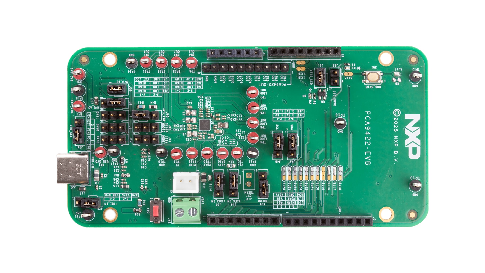
2.2 Board Description
Overview of the PCA9422 board.
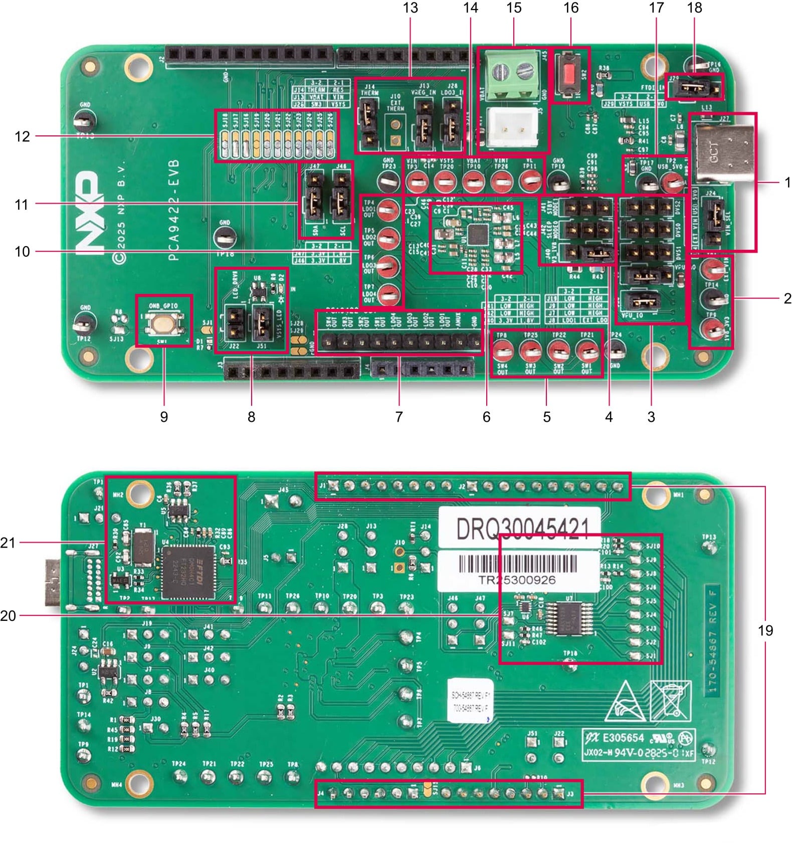
Table 1. Board Description.
| Number | Block | Description |
|---|---|---|
| 1 | USB-C input | 5 V USB power supply and communication port for PCA9422B |
| VIN_SEL | Vin selection, 5 V from external power supply or from USB | |
| 2 | Ext PS | External 5 V supply input |
| Ext LDO | On board LDO output voltage test point | |
| 3 | DVS_CTRL | Logic voltage selection for DVS0, DVS1 and DVS2 |
| Voltage pull ups | Voltage Logic and voltage level selection for interrupts, run modes, DVS and I²C | |
| 4 | RUN mode sel | Run mode selection via SLEEP_MODE0 and STBY_MODE1 pins |
| Ext LDO vout sel | On board LDO output voltage selection | |
| 5 | BUCKs vout | SW1-SW4 output voltage test points |
| 6 | PMIC | PCA9422 PCB footprint area |
| 7 | PMIC_OUT | Header with AMUX and all regulator's output |
| 8 | LEDs | Jumpers for VSYS LED and LED_DRVR |
| 9 | SWITCH1 |
Puss button connected to ON pin |
| 10 | LDOs vout | LDO1-LDO4 output voltage test points |
| 11 | SDA and SCL Voltage | Voltage level selection I²C lines (3.3 V or 1.8 V) |
| 12 | FT_AR | Solder jumpers for FTDI chip or Arduino selection |
| 13 | VREG_IN, LDO3_IN | Input selection for external LDO (VBAT or USB_5V0) and LDO3_IN (VSYS or SW3_OUT) |
| THERM | Thermistor or resistor selection | |
| 14 | System voltages | VIN, VBAT, VSYS and internal voltages (VIN, VL) test points |
| 15 | VBAT inputs | Connection options for a battery cell |
| 16 | SWITCH2 |
Puss button connected FTDI reset pin |
| 17 | USB_5V0 | USB-C output voltage test point |
| 18 | FTDI_IN | VSYS/5 V USB input selection jumper for FTDI and ADC circuit blocks |
| 19 | FRDM/ARDUINO conn | I/O header compatible with NXP Freedom and Arduino UNO boards |
| 20 | ADC sensing | ADC area and solder jumpers for regulators and signal monitoring |
| 21 | FTDI USB to I²C comm | On board USB to I²C communication circuitry |
3. Configure Hardware
3.1 Configure the Hardware
Figure 2 presents a typical hardware configuration incorporating the development board, power supply and Windows PC workstation.
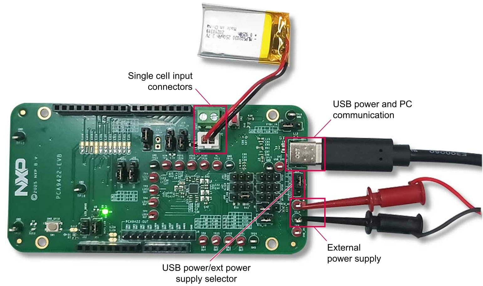
Connect wires on the following pins as shown in Figure 2, and make sure that the power supply is turned off during the wiring stage:
- A Li-ion battery – Connect to VBAT test point or connectors
- VIN Input – Powered by USB-C connector or external power supply
Figure 3 shows the location of jumpers on the evaluation board.
Table 2. Jumper description and default setting.
| Jumper | Description | Setting | Connection/Result |
|---|---|---|---|
J24 |
VIN selection | [1-2] | USB power input |
| [2-3] | External power supply input | ||
J8 |
INTB, SYSRSTn and Run mode pull-up voltage selection | [1-2] | Pullup to external LDO (3.3 V or 1.8 V) |
| [2-3] | Pullup to LDO1_OUT | ||
J30 |
I²C and DVS pins pull up voltage | Closed | Pullup to LDO2_OUT |
J40 |
External LDO voltage selection | [1-2] | 1.8 V |
| [2-3] | 3.3 V | ||
J41 |
Logic configuration for STBY_MODE1 | [1-2] | Logic high |
| [2-3] | Logic low | ||
J42 |
Logic configuration for SLEEP_ MODE0 | [1-2] | Logic high |
| [2-3] | Logic low | ||
J6 |
Voltage monitoring header for all regulators, including AMUX | – | Pin assignation: |
| 1: BUCK-BOOST output | |||
| 2: BUCK3 output | |||
| 3: BUCK2 output | |||
| 4: BUCK1 output | |||
| 5: LDO4 output | |||
| 6: LDO3 output | |||
| 7: LDO2 output | |||
| 8: LDO1 output | |||
| 9: AMUX | |||
| 10: GND | |||
J51 |
System voltage LED | Closed | System status indicator LED |
J22 |
LED driver | Open | Close jumper to make LED driver available |
J46 - J47 |
SCL/SDA level voltage selection | [1-2] | 1.8 V Logic |
| [2-3] | 3.3 V Logic | ||
SJ16 - SJ26 |
FTDI or FRDM/Arduino selection | [1-2] | Connects signal to onboard FTDI |
| [2-3] | Connects signal to FRDM/Arduino | ||
J14 |
Thermistor/Resistor selection | [1-2] | Connects to 10 K onboard resistor |
| [2-3] | Connects to 10 K onboard thermistor | ||
J13 |
On board LDO input selection | [1-2] | Selects VIN as input |
| [2-3] | Selects VBAT as input | ||
J28 |
LDO3 input selection | [1-2] | Selects SW3_OUT as input |
| [2-3] | Selects VSYS as input | ||
J45 |
Battery connection | – | Power connector for VBAT (high current testing) |
J51 |
Battery connection | – | Connector header for VBAT (common in battery cells) |
J19, J9, J7 |
DVS0-DVS2 logic level selection | [1-2] | Logic high |
| [2-3] | Logic low | ||
J29 |
FTDI/ADC input voltage selection | [1-2] | Selects USB_5V0 as input |
| [2-3] | Selects VSYS as input | ||
J1-J4 |
I/O header | – | I/O header compatible with NXP Freedom and Arduino |
SJ1 - SJ11 |
ADC voltage and signals monitoring | Closed | Open connection to reduce standby current consumption |
Design Resources
Board Documents
Available to selected customers only; a nondisclosure agreement (NDA) is required. Contact your local NXP sales representative for more information.
Additional References
In addition to our PCA9422 page, you may also want to visit: