Getting Started with the PCA9452A-EVK
Contents of this document
-
Out of the Box
-
Get the Hardware
-
Install Software
-
Configure Hardware
Sign in to save your progress. Don't have an account? Create one.
Purchase your PCA9452A-EVK
1. Out of the Box
The NXP analog product development boards provide an easy-to-use platform for evaluating NXP products. The boards support a range of analog, mixed-signal and power solutions. They incorporate monolithic integrated circuits and system-in-package devices that use proven high-volume technology. NXP products offer longer battery life, a smaller form factor, reduced component counts, lower cost and improved performance in powering state-of-the-art systems.
This page will guide you through the process of setting up and using the PCA9452A-EVK evaluation board.
1.1 Kit Contents/Pack list
The kit contents include:
- Assembled and tested evaluation board in an antistatic bag
- 1x Interface (FTDI C232HM-DDHSL-0) cable, which serves as a USB to I²C interface between the computer and the PCA9452A-EVK evaluation board
- Quick Start Guide
1.2 Additional Hardware
In addition to the kit contents, the following hardware is necessary when working with this board.
- Power supply with a range of 3.0 V to 5.0 V and a current limit set initially to 1.0 A (maximum current consumption can be up to 7.0 A)
- Oscilloscope/multimeter
- Electronic load (optional) - each power rail output can be connected to e-load for testing
2. Get to Know the Hardware
2.1 Board Features
-
Six buck regulators
- One 6 A buck regulator with DVS (BUCK1 and BUCK3 are in Dual Phase)
- One 3 A buck regulator with DVS
- One 3 A buck regulator
- Two 2 A buck regulators
-
Five linear regulators
- Two 10 mA LDOs
- One 150 mA LDO
- One 200 mA LDO
- One 300 mA LDO
- 32.768 kHz crystal oscillator driver and buffer output
- Two-channel logic level translator
-
System features
- 2.85 V to 5.5 V operating input voltage range
- Power ON/OFF control
- Standby/run mode control
- Smart DVS control
- Interrupt configuration
- Fm+ 1 MHz I²C Interface (via FTDI USB to I²C cable)
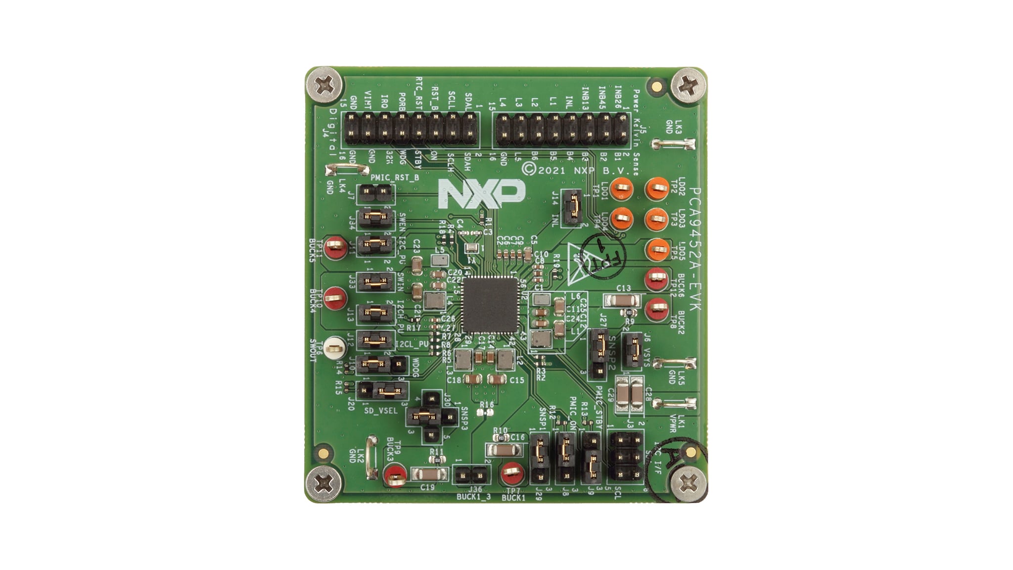
2.2 Board Description
This evaluation board features the PCA9452A power management IC. The kit integrates all hardware needed to fully evaluate the PMIC. It integrates a communication bridge based on FTDI to interface with the PCA9452A GUI software interface to fully configure and control the PMIC.
2.3 Board Components
Identify the different main components of the board.
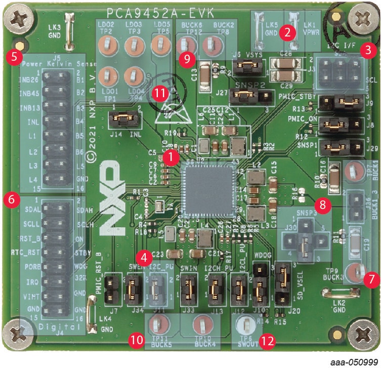
- PCA9452A PMIC
- VPWR and GND input power connectors
- I²C connector
- I²C pull up voltage jumper (I2C_PU)
- Kelvin sense connector
- Digital IO connector
- BUCK1 and BUCK3 output test points
- BUCK3 Feedback connection
- BUCK2 and BUCK6 output test points
- BUCK4 and BUCK5 output test points
- Load switch output test point
3. Install Software
Installing software is necessary to work with this evaluation board.
- Go to: PCA945A-EVK
- Extract the zip file PCA9452_EVB_GUI.zip into selected folder. No need to install. (if password is asked during unzip, then type “NXP”)
- Install the FTDI cable driver from website D2XX Drivers
- Run the file PCA9452.exe. The interface window is shown below
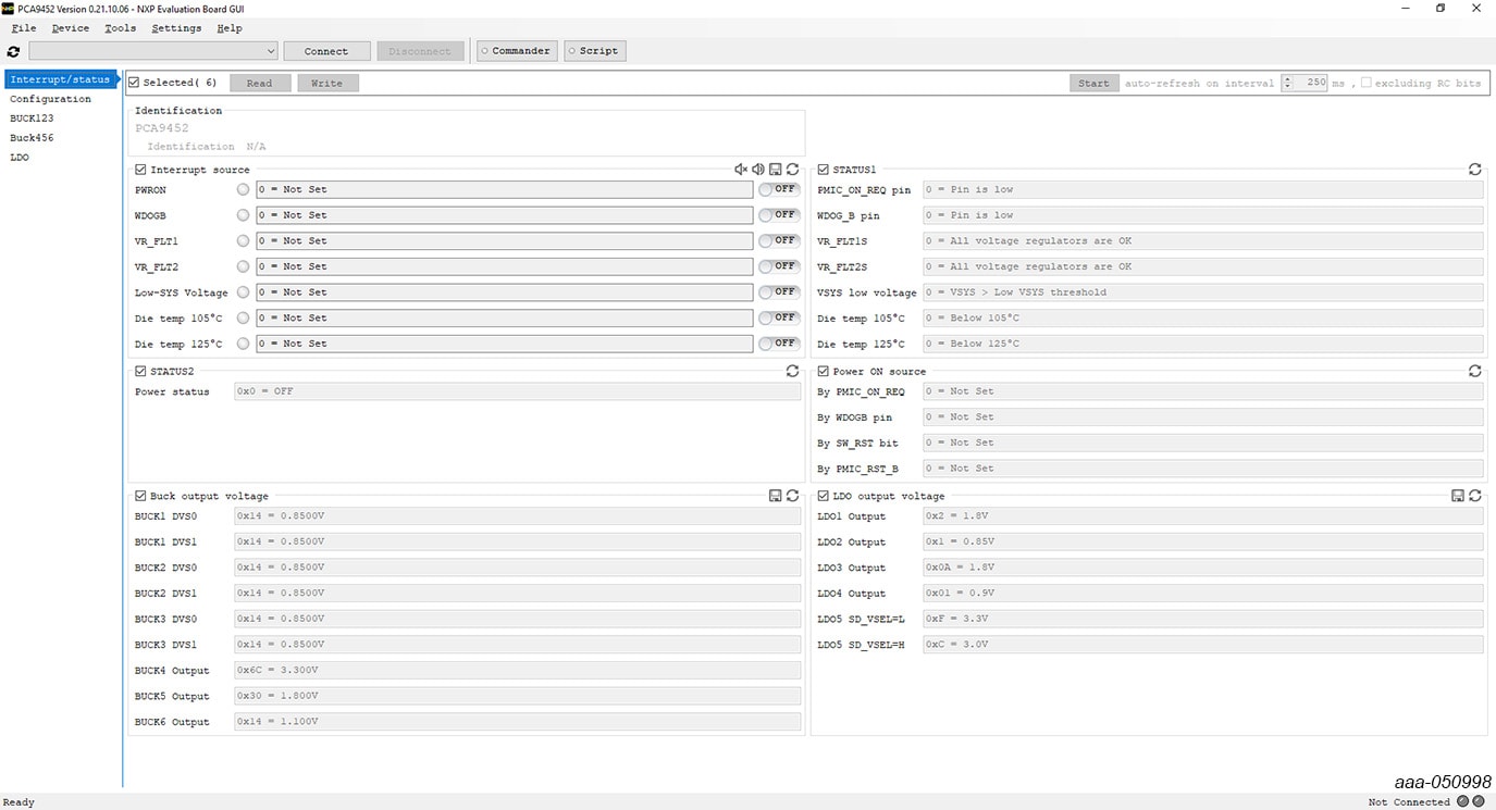
3.1 GUI Setup
After turning on the power supply and plugging in the USB part of the FTDI cable, the GUI detects the cable automatically. Select the cable type (FT2TRWH9) from the drop-down menu, and then click “Connect” button.
On the “Device connection status” section (right bottom part of the screen), the GUI shows “Connected” with green light.
4. Configure the Hardware
PCA9452A-EVK Test Setup

4.1 Evaluation Board Connection
PCA9452A-EVK Connections
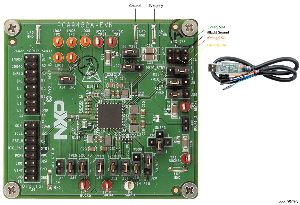
4.2 Configure and Power the Board
- Connect the wires of the FTDI cable on the following pins as shown in Figure 4, and make sure the Connect both SDAs, SCL, GND, and the 3.3 V wires from the FTDI cable as mentioned in Figure 4 above
-
Connect both SDAs, SCL, GND, and the 3.3 V wires from the FTDI cable as mentioned in Figure 4 above
- SCL serial clock signal (orange cable) should be connected to pin 5 of the 'Digital IO' connector (
J3). - Both SDA serial data wires (yellow and green cables) should be connected to create bidirectional data. Connect yellow cable to pin 3, and green cable to pin 4 of the 'Digital IO' connector (
J3). - GND ground signal (black cable) should be connected to pin 6 or pin 2 of the 'Digital IO' connector (
J3). - Remove jumper from
J11. 3.3 V supply wire (red cable) from FTDI cable should be connected to pin 2 of the 'I2C_PU' connector (J11).
- SCL serial clock signal (orange cable) should be connected to pin 5 of the 'Digital IO' connector (
- With the power supply turned off, connect 5 V power supply to LK1 connector and corresponding ground to LK5
- Turn ON power supply.
- Connect USB connector of the FDTI cable to PC.
Power supply is turned off and the USB connector is disconnected during the wiring stage:
Design Resources
Board Information
Additional References
In addition to our PCA9452: PCA9452 Power Management IC for i.MX 93x Auto Processor page, you may also want to visit:
Application pages: Application page: Driver Monitoring Systems (DMS) and Occupant Monitoring Systems