Getting Started with the PF9453 QFN Evaluation Board
Contents of this document
-
Out of the Box
-
Get Hardware
-
Configure Hardware
Sign in to save your progress. Don't have an account? Create one.
Purchase your PF9453AHN-EVB
1. Out of the Box
The NXP analog product development boards provide an easy-to-use platform for evaluating NXP products. The boards support a range of analog, mixed-signal and power solutions. They incorporate monolithic integrated circuits and system-in-package devices that use proven high-volume technology. NXP products offer longer battery life, a smaller form factor, reduced component counts, lower cost and improved performance in powering state-of-the-art systems.
This page will guide you through the process of setting up and using the PF9453 QFN evaluation board.
1.1 Kit Contents and Packing List
The kit contents include:
- Assembled and tested the evaluation board in an antistatic bag
- Quick Start Guide
1.2 Additional Hardware
In addition to the kit contents, the following hardware is necessary or beneficial when working with this board.
- Power supply with a range of 2.7 V to 5.0 V and a current limit set initially to 1.0 A (maximum power consumption at default voltages can be up to 22 W)
- Oscilloscope/multimeter
- Electronic load (optional) - each power rail output can be connected to electronic load for testing
1.3 Minimum System Requirements
This evaluation board requires a Windows PC workstation. Meeting these minimum specifications should produce great results when working with this evaluation board:
- USB-enabled computer with Windows 7, Windows 8 or Windows 10
1.4 Software
Installing software is necessary to work with this evaluation board. All listed software is available on the PF9453 QFN Evaluation Board information page or from the provided link.
- Go to PF9453 EVB graphical user interface
- Extract the Evaluation Kit GUI zip file, PF9453_EVB_GUI_1.25.2.21-x64, into the selected folder. No need to install. (If the password is requested to unzip, type “NXP”)
- Install the FTDI D2XX direct drivers from the FTDI Chip page
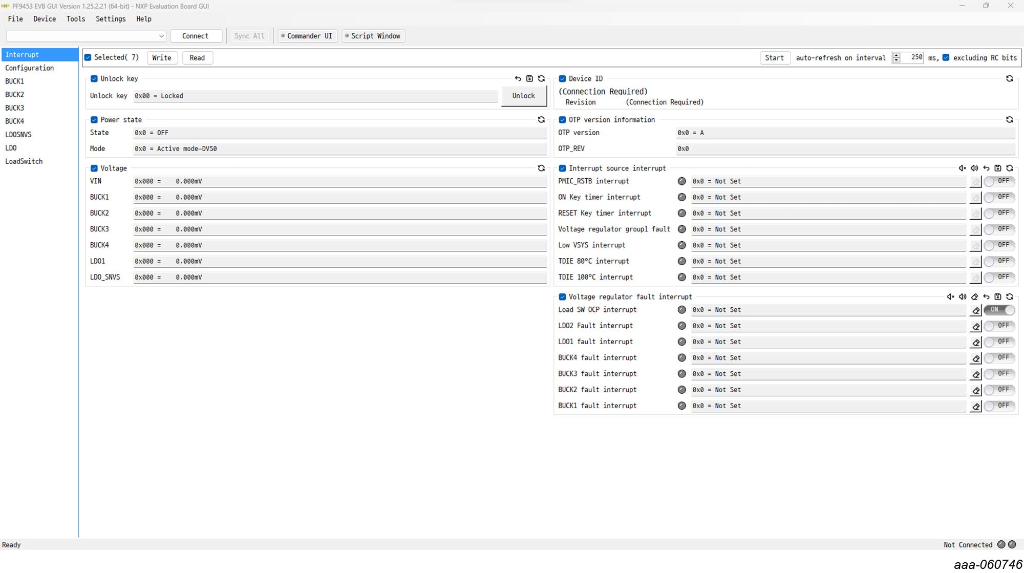
- Run the file PF9453.exe. The interface window is shown in Figure 1
2. Get Hardware
2.1 Board Features
-
Four BUCK regulators:
- One 2.7 A BUCK regulator with DVS
- Two 2 A BUCK regulators
- One 2.5 BUCK regulator
-
Three linear regulators:
- One 10 mA LDO
- One 250 mA LDO
- One 200 mA LDO
- 400 mA load switch with a built-in active discharge resistor
- 32.768 kHz crystal oscillator driver and buffer output
-
System features:
- 2.7 V to 5.5 V operating input voltage range
- Power ON/OFF control
- Standby/Deep Standby/Run mode control
- Interrupt configuration
- Fm+ 1 MHz I²C interface (via FTDI USB to I²C IC)
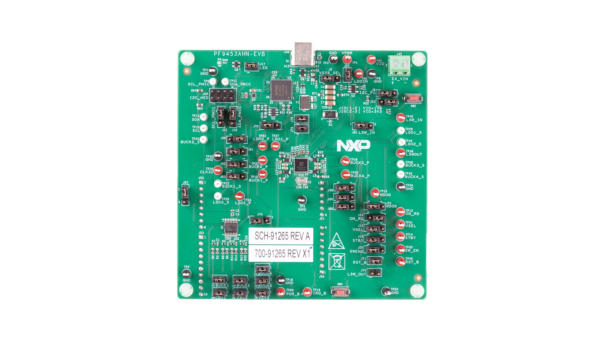
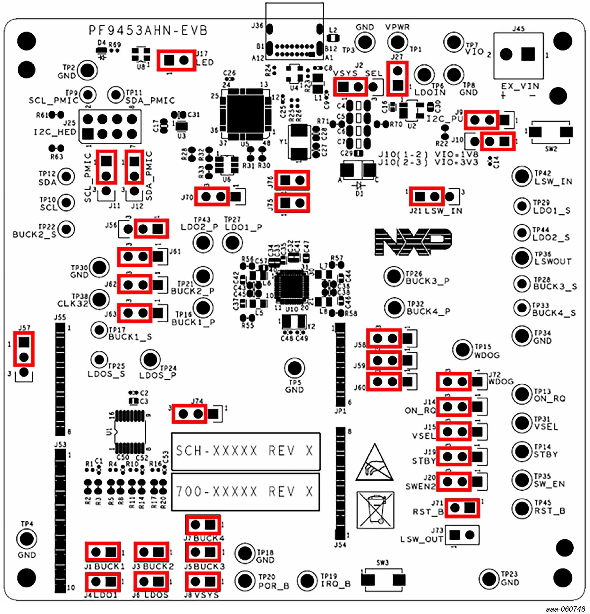
2.2 Board Description
Overview of the PF9453 board.
| Name | Default | Description |
|---|---|---|
J1 |
CLOSED | Connects BUCK1_OUT voltage to ADC0 channel |
J2 |
1 to 2 |
Select source voltage for VSYS and PSYS (PMIC input voltage):
|
J3 |
CLOSED | Connects BUCK2_OUT voltage to ADC1 channel |
J4 |
CLOSED | Connects LDO1_OUT voltage to ADC4 channel |
J5 |
CLOSED | Connects BUCK3_OUT voltage to ADC2 channel |
J6 |
CLOSED | Connects LDO_SNVS voltage to ADC5 channel |
J7 |
CLOSED | Connects BUCK4_OUT voltage to ADC3 channel |
J8 |
CLOSED | Connects PSYS voltage to ADC6 channel |
J9 |
2 to 3 |
Select source voltage for VIO (Voltage for input and output signals):
|
J10 |
1 to 2 |
Select output voltage of the external LDO (U2):
|
J11 |
1 to 2 |
Select if SCL_PMIC signal (PMIC I²C signal) passes through the level shifter (U3) or not:
|
J12 |
1 to 2 |
Select if SDA_PMIC signal (PMIC I²C signal) passes through the level shifter (U3) or not:
|
J14 |
2 to 3 |
Select PMIC_ON_REQ level:
|
J15 |
2 to 3 |
Select SD_VSEL level:
|
J17 |
CLOSED | Connects the green LED driver (U8) to PSYS voltage |
J19 |
2 to 3 |
Select PMIC_STBY_REQ level:
|
J20 |
2 to 3 |
Select LSW_EN level:
|
J21 |
1 to 2 |
Select load-switch input voltage:
|
J27 |
CLOSED | Connects the external LDO (U2) to PSYS voltage |
J56 |
1 to 2 |
Select an SCL connection:
|
J57 |
1 to 2 |
Select an SDA connection:
|
J58 |
2 to 3 |
Select if PMIC_ON_REQ connection:
|
J59 |
2 to 3 |
Select if PMIC_STBY_REQ connection:
|
J60 |
2 to 3 |
Select if WDOG_B connection:
|
J61 |
2 to 3 |
Select if IRQ_B connection:
|
J62 |
2 to 3 |
Select if POR_B connection:
|
J63 |
2 to 3 |
Select if LSW_EN connection:
|
J70 |
2 to 3 |
Select if SD_VSEL connection:
|
J71 |
CLOSED | Connects PMIC_RET_B to the reset button (SW3) |
J72 |
2 to 3 |
Select WDOG_B (watchdog reset input) signal:
|
J73 |
OPEN | Jumper for internal validation only |
J74 |
2 to 3 |
Select if PMIC_RST_B connection:
|
J75 |
CLOSED | Connects LDO1 input voltage (INL1) to PSYS |
J76 |
CLOSED | Connects LDO2 input voltage (INL2) to PSYS |
3. Configure Hardware
3.1 Configure Hardware
Figure 3 presents a typical hardware configuration incorporating the development board, power supply and Windows PC workstation.
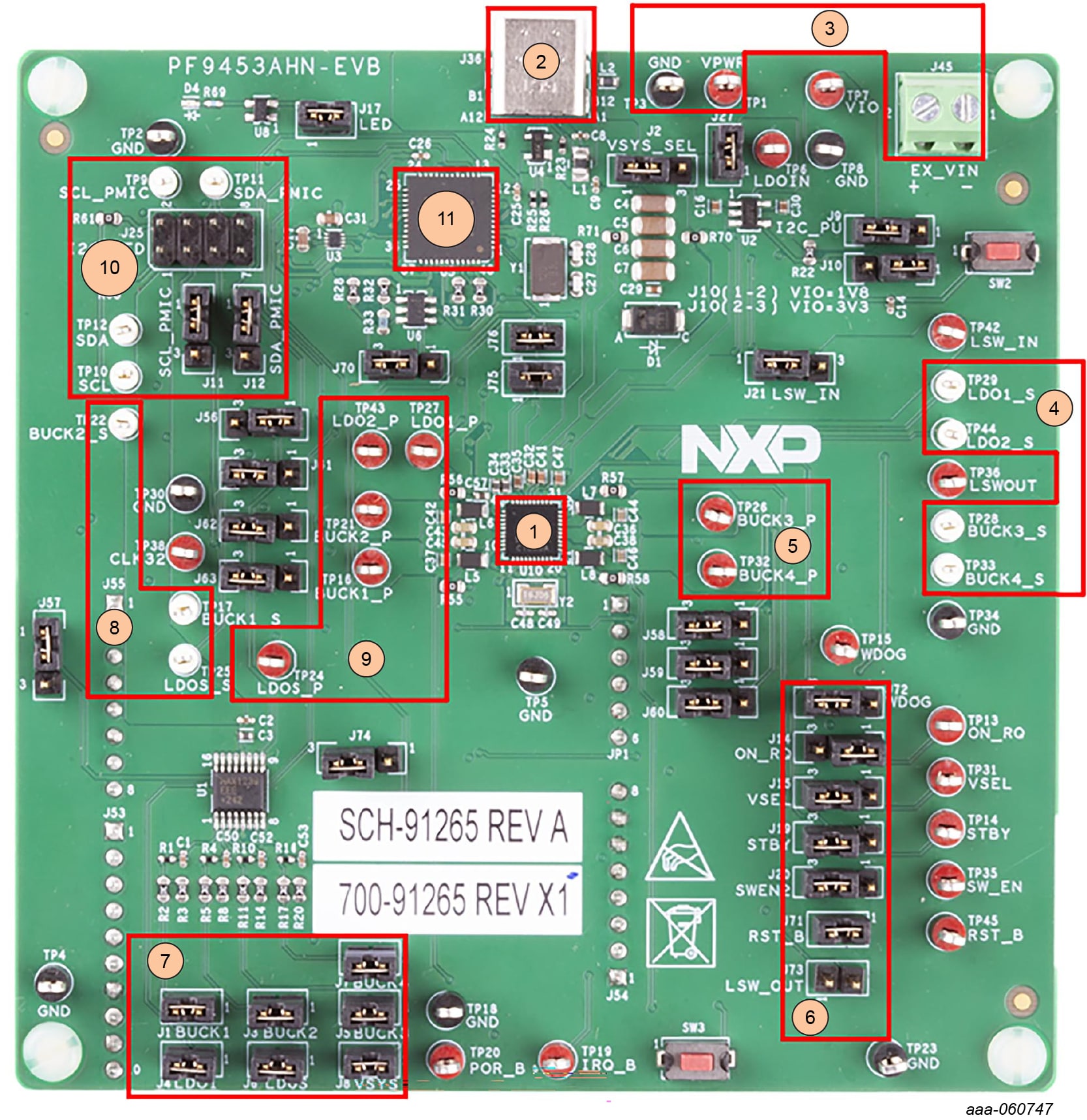
- PF9453 PMIC (QFN package)
- USB-Type C connector
- VPWR and GND input power connectors
- LDO1, LDO2, BUCK3 and BUCK4 sensing test points
- BUCK3 and BUCK4 power test points
- Digital signals jumper selectors
- ADC jumpers
- BUCK1, BUCK2 and LDO_SNVS sensing test points
- LDO1, LDO2, LDO_SNVS, BUCK2 and BUCK1 power tests points
- I²C headers and tests points
- FTDI (I²C to USB IC)
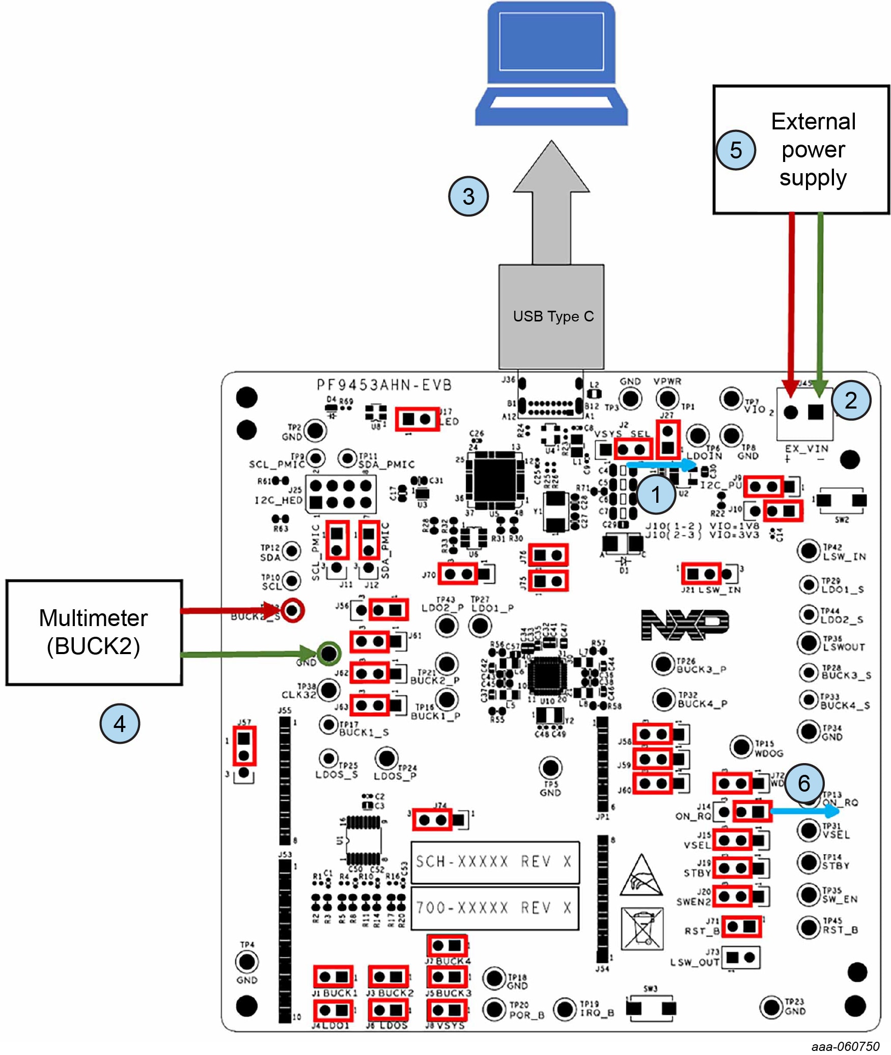
Refer to Figure 3 and follow the next steps to test the PF9453 QFN – EVB. Make sure that all jumpers are in the default positions before starting. (See section Section 2.2) and no other cables are connected to the PF9453 QFN – EVB:
- Connect the positive terminal of the multimeter to TP22 (BUCK2_OUT) test point and the negative terminal of the multimeter to TP30 GND test point, see Figure 3 where step 1 is represented with the circle with number 1
- Connect the USB-Type C to the PF9453 QFN –EVB. See that the green LED D4 is ON, refer, circle with Figure 3 number 2. Note: With this configuration, we are using the USB-Type C connector as the power supply. Consider not connecting loads that may demand more power than the USB-Type C supply can deliver. If tests that could demand more current that the USB-Type C power supply allows must be done, that is, efficiency tests, it is recommended to use an external power supply. For more details about how to set up, see below: Using an external power supply. If the USB-Type C power supply is enough, continue with the next step/li>
- Move the
J14to positionJ14(1 to 2), refer to Figure 3, circle with number 3 (this turns on the PMIC by setting the high state the PMIC_ON_REQ pin) - Measure the default voltage of BUCK2 in the multimeter, must be 0.85 V (default voltage)
Follow the next steps to start testing the PF9453 QFN – EVB with an external power supply. Before starting make sure that all jumpers are in the default position. (See section Section 2.2) and no other cables are connected to the PF9453 QFN – EVB:
- Move the
J2jumper to positionJ2(2 to 3). Input PMIC voltage from an external power supply, see Figure 4. Step 1 is represented with the circle with number 1 - Connect the external power supply to the
J45connector: positive terminal toJ45(pin 2), negative terminalJ45(pin 1) see Figure 4, circle with number 2. The external power supply can also be connected to the following tests points: positive terminal to TP1 (VPWR) and negative terminal to TP3 (GND) - Connect the USB-Type C to the PF9453-EVB, see Figure 4, circle with number 3
- Connect the positive terminal of the multimeter to TP22 (BUCK2_OUT) test point and the negative terminal of the multimeter to TP30 (GND) test point. See Figure 5, circle with number
- Configure the power supply to 5.0 V, 1 A, and turn it on. See that the green LED D4 is ON, see the Figure 4, circle with number 5
- Move the
J14Jumper to positionJ14(1 to 2), see Figure 4, circle with number 6. (This turns on the PMIC by setting the high state the PMIC_ON_REQ pin) - Measure the default voltage of BUCK2 in the multimeter, you see 0.85 V (default voltage)
Design Resources
Board Information
Additional References
In addition to our PF9453 product page, you may also want to visit: