Technical content and expertise to help jump start your design and get you to production faster.
Start your designDownload our latest development and embedded software solutions.
Expedite time-to-market with our extensive lineup of development kits.
Jump-start your design with proven hardware and software solutions.
Get the latest specifications in our technical documentation library.
Further your technical expertise with online and in-person instruction.
Get comprehensive paid support to fast-track your product development.
Design ideas, demo videos, quality answers. Connect with NXP professionals and other knowledgeable designers ready to help.
Software, documentation, evaluation tools. The resources to build comprehensive solutions and accelerate your time to market.
Access our design resource libraryWe're always looking for passionate and talented people to work with us.
Join our teamArchived content is no longer updated and is made available for historical reference only.
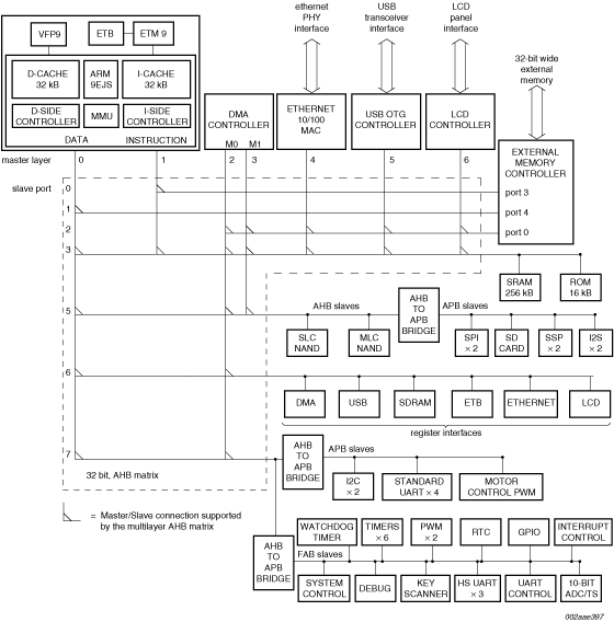
The LPC3230 operates at CPU frequencies of up to 266 MHz. The NXP® implementation uses an ARM926EJ-S CPU core with a Harvard architectur, 5-stage pipeline, and an integral Memory Management Unit (MMU). The LPC3230 also includes 256 kB of on-chip static RAM, a NAND flash interface, an LCD controller that supports STN and TFT panels, and an external bus interface that supports SDR and DDR SDRAM, as well as static devices. In addition, the LPC3230 includes a USB 2.0 full-speed interface, seven UARTs, two I2C-bus interfaces, two SPI/SSP ports, two I2S-bus interfaces, two single output PWMs, a motor control PWM, six general purpose timers with capture inputs and compare outputs, a Secure Digital (SD) interface, and a 10-bit Analog-to-Digital Converter (ADC) with a touch screen sense option.