Technical content and expertise to help jump start your design and get you to production faster.
Start your designDownload our latest development and embedded software solutions.
Expedite time-to-market with our extensive lineup of development kits.
Jump-start your design with proven hardware and software solutions.
Get the latest specifications in our technical documentation library.
Further your technical expertise with online and in-person instruction.
Get comprehensive paid support to fast-track your product development.
Design ideas, demo videos, quality answers. Connect with NXP professionals and other knowledgeable designers ready to help.
Software, documentation, evaluation tools. The resources to build comprehensive solutions and accelerate your time to market.
Access our design resource libraryWe're always looking for passionate and talented people to work with us.
Join our teamArchived content is no longer updated and is made available for historical reference only.
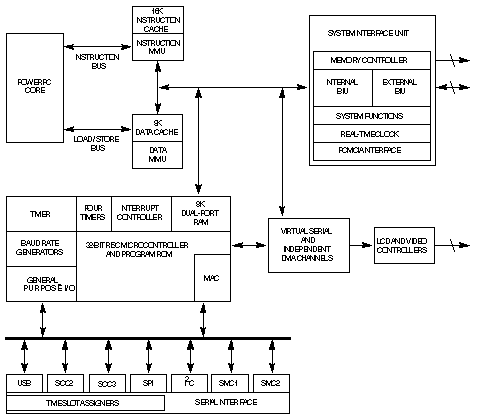
The MPC823e microprocessor is a versatile, one-chip integrated microprocessor and peripheral combination that can be used in a variety of electronic products. It particularly excels in low-power, portable, image capture and personal communication products. It is a version of the MPC823 microprocessor that provides enhanced performance with larger data and instruction caches. Like the MPC823, it has a universal serial bus (USB) interface and video display controller, as well as the existing LCD controller of the MPC823 (Rev A) device.
The MPC823e microprocessor integrates a high-performance embedded MPC8xx core with a communication processor module that uses a specialized RISC processor for imaging and communication. The communication processor module can perform embedded signal processing functions for image compression and decompression. It also supports seven serial channels--two serial communication controllers, two serial management controllers, one I²C port, one USB channel, and one serial peripheral interface.
This two-processor architecture consumes power more efficiently than traditional architectures because the communication processor module frees the core from peripheral tasks like imaging and communication.
Embedded MPC8xx Core Provides 99MIPS (Using Dhrystone 2.1) or 172K Dhrystones 2.1 at 75MHz
Architecture
The MPC823e microprocessor uses a dual-processor architecture design approach with large data and instruction caches to provide high-performance using a general-purpose RISC integer processor and a special-purpose 32-bit scalar RISC communication processor module. The peripherals are uniquely designed for communication requirements and can provide embedded signal processing functions for communication and user interface enhancements and the I/O support needed for high-speed digital communication.
The MPC823e is comprised of four main modules that interface with the 32-bit internal bus:
Embedded MPC8xx Core
The MPC8xx core is built on Power Architecture technology. It has a fully static design that consists of an integer block, hardware multiplier/divider block and a load/store block. The core supports integer operations on a 32-bit internal data path and 32-bit arithmetic hardware. Its interface to the internal and external buses is 32 bits. The core uses a two-instruction load/store queue, four-instruction prefetch queue, and a six-instruction history buffer. It performs branch folding and branch prediction with conditional prefetch, but without conditional execution. With single bus cycles, the core can operate on 32-bit external operands and with critical-word-first in multiple bus cycles. The integer block supports 32 x 32-bit fixed-point general-purpose registers and can execute one integer instruction per clock cycle.
The MPC8xx core is integrated with the memory management units, an instruction cache, and a data cache. The memory management units provide 32-entry, fully associative instruction and data TLBs, with multiple page sizes of 4K (1K protection), 16K, 512K, and 8M. They support 16 virtual address spaces and 16 protection groups. Special registers are available to support software tablewalk and update.
The instruction cache is 16K, four-way, set-associative with physical addressing. It allows single-cycle accesses on hit with no added latency for miss. It is four words per line and supports burst line fill using an LRU replacement algorithm. The cache can be locked on a line basis for application critical routines. The data cache is 8K, two-way, set-associative with physical addressing. It allows single-cycle accesses on hit with one added clock latency for miss. It has four words per line and supports burst line fill using an LRU replacement algorithm. The cache can be locked on a line basis for application critical data and can be programmed to support copyback or writethrough mode via the memory management unit. The cache-inhibit mode can be programmed per MMU page. The MPC8xx core, with its instruction and data caches, can deliver approximately 99MIPS at 75MHz (using Dhrystone 2.1) or 172K Dhrystones, based on the assumption that it is issuing one instruction per cycle with a cache hit rate of 94%.
Communication Processor Module
The communication processor module contains features that allow the MPC823 microprocessor to excel in imaging, personal communication, and low-power applications. These features are divided into three categories:
The MPC823e embedded DSP function allows the communication processor module to execute imaging algorithms in parallel with the MPC8xx core to achieve maximum performance with very little power. The DSP can execute one 16x16 MAC on every clock cycle. It has preprogrammed filtering functions like FIR, MOD, DEMOD, IIR, and downloadable imaging functions for JPEG® image compression and decompression.
The robust communication features of the MPC823e are provided by the communication processor module. These features include a RISC microcontroller with multiply accumulate hardware, two serial communication controllers, two serial management controllers, eight dedicated serial channels for the Universal Serial Bus, one inter-integrated circuit port, one serial peripheral interface, an 8K dual-port RAM, interrupt controller, two time-slot assigners, and four independent baud rate generators.Twenty serial DMA channels support the SCCs, SMCs, USB channel, SPI, and I2C controllers. The independent DMAs give you two channels for general-purpose DMA usage. They offer high-speed transfers, 32-bit data movement, buffer chaining, and independent request and acknowledge logic. The RISC microcontroller is the only block that can access the IDMA registers directly. The CPU can only access them indirectly via a buffer descriptor.
System Interface Unit
The system interface unit supports traditional 68K big-endian memory systems, traditional x86 little-endian memory systems, and modified little-endian memory systems. It also provides power management functions, reset control, a decrementer, timebase, and real-time clock based on Power Architecture technology. Although the MPC8xx core is a 32-bit device internally, it can be configured to operate with an 8-, 16-, or 32-bit data bus. Regardless of the system bus size, dynamic bus sizing is supported, which allows 8-, 16-, and 32-bit peripherals and memory to coexist on a 32-bit system bus.
The memory controller supports as many as eight memory banks with glueless interfaces to DRAM, SRAM, EPROM, Flash EPROM, SDRAM, EDO and other peripherals with two-clock initial access to external SRAM and bursting support. It provides variable block sizes between 32K and 256M. The memory controller has 0 to 20 wait states for each bank of memory and can use address-type matching to qualify each memory bank access. It provides four byte-enable signals for varying width devices, one output-enable signal, and one boot chip-select that is available at reset.
The DRAM interface supports 8-, 16-, and 32-bit ports and uses a programmable state machine to support almost any memory interface. Memory banks can be defined in depths of 256K, 512K, 1M, 2M, 4M, 8M, 16M, 32M, or 64M for all port sizes. In addition, the memory depth can be defined as 64K and 128K for 8-bit memory or 128M and 256M for 32-bit memory. The DRAM controller supports page mode access for successive transfers within bursts. The MPC823e supports a glueless interface to one bank of DRAM, while external buffers are required for additional memory banks. The refresh unit provides CAS before RAS, a programmable refresh timer, refresh active during external reset, disable refresh modes, and stacking for a maximum of seven refresh cycles.
Video/LCD Controller
The MPC823e has a dual-purpose video/LCD controller that shares common dual-port memory. However, only one of the controllers can be run at a time.
The video controller can be used to drive a digital NTSC/PAL encoder or a wide variety of digital LCD panels. The frame buffer is stored in system memory in the form of an orthogonal matrix--rows and columns. The 24-bit color data is organized as pixel components whether it is sequential RGB or YCrCb. Each pixel component is represented by a byte. The video controller uses a dedicated DMA channel to read the display data from the frame buffer and drive it to the video interface. It also generates the required timing signals, such as horizontal sync, vertical sync, field, and blanking.
The LCD controller provides extremely versatile LCD support for 8-bit color, monochrome or 4/16-level grayscale, color TFT (12 bits, 4x3 RGB), and passive color (xSTN) 4/8 bit data. The controller supports 4- or 8-bit single-scan, 2+2 bit dual-scan, or 4+4 bit dual-scan. It is programmable for frame rate, number of pixels per line, and number of lines per frame. The panel voltage is programmable through the duty cycle for contrast adjustments implemented in the communication processor module program. Display data is stored in memory space and is transferred into the controller using the DMA channel.
PCMCIA-ATA Controller
The PCMCIA-ATA interface is a leader controller that is compliant with Version 2.1 of the PCMCIA standard. The interface supports one independent PCMCIA socket with the required external transceivers or buffers. It provides eight memory or I/O windows that can be allocated to the socket. If the PCMCIA port is not being used as a card interface, it can provide eight general-purpose pins and two output-only pins with interrupt capability.
Power Management
The MPC823e microprocessor supports a wide range of power management features, including normal high, normal low, doze, sleep, deep-sleep, and power-down modes. In normal high mode, the MPC823e is fully powered with all internal units operating at the full speed of the processor. Normal low mode is the same as normal high, except it operates at a much lower frequency. There is a doze mode determined by a clock divider that allows the operating system to reduce the operational frequency of the processor.
Doze mode disables core functional units except the timebase, decrementer, PLL, memory controller, real-time clock, LCD controller, and communication processor module. Sleep mode is a lower power mode that disables everything except the real-time clock, timebase, decrementer, and periodic interrupt timer, thus leaving the PLL active for quick wake-up. The deep-sleep mode then disables the PLL for lower power, but slower wake-up. Power-down mode disables all logic in the processor, except the minimum logic required to restart the device. It saves the most power, but requires the longest wake-up time.
System Debug Support
The MPC823e microprocessor contains an advanced debug interface that provides superior debug capabilities without any loss of speed. It supports six watchpoint pins that can be combined with eight internal comparators, four of which operate on the effective address of the address bus. The other four comparators are split--two comparators operate on the effective address on the data bus and two comparators operate on the data on the data bus. The MPC823 microprocessor can compare using the =, <, and />conditions to generate watchpoints. Each watchpoint can then generate a breakpoint that can be programmed to trigger in a programmable number of events.
Applications
The MPC823e microprocessor is specifically designed to be a general-purpose, low-cost entry point to the NXP® embedded processor family for systems in which advanced GUIs, communications, and high-level real-time operating systems are used. The device excels in applications that require the performance of a single-issue MPC8xx core with an ample amount of data and instruction cache. It provides all the basic features of glueless memory connections along with highly functional serial connectivity, a graphical LCD, and a video display controller. The MPC823e excels in low-power and portable applications because of its extensive power-down modes and low normal operation current.