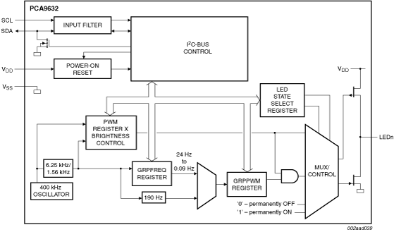
The PCA9632 is an I²C-bus controlled 4-bit LED driver optimized for Red/Green/Blue/Amber (RGBA) color mixing applications. The PCA9632 is a drop-in upgrade for the PCA9633 with 40× power reduction. In Individual brightness control mode, each LED output has its own 8-bit resolution (256 steps) fixed frequency Individual PWM controller that operates at 1.5625 kHz with a duty cycle that is adjustable from 0 % to 99.6 % to allow the LED to be set to a specific brightness value. In group dimming mode, each LED output has its own 6-bit resolution (64 steps) fixed frequency Individual PWM controller that operates at 6.25 kHz with a duty cycle that is adjustable from 0 % to 98.4 % to allow the LED to be set to a specific brightness value. A fifth 4-bit resolution (16 steps) Group PWM controller has a fixed frequency of 190 Hz that is used to dim all the LEDs with the same value.
While operating in the Blink mode, each LED output has its own 8-bit resolution (256 steps) fixed frequency Individual PWM controller that operates at 1.5625 kHz with a duty cycle that is adjustable from 0 % to 99.6 % to allow the LED to be set to a specific brightness value. Blink rate is controlled by the Group frequency setting that has an 8-bit resolution (256 steps). The blink rate is adjustable between 24 Hz and once every 10.73 seconds. For Group frequency settings between 6 Hz and 24 Hz, the Group PWM has a 6-bit resolution (64 steps) with a duty cycle that is adjustable from 0 % to 98.4 %. For Group frequency settings between 6 Hz and 0.09 Hz (once in 10.73 seconds), the Group PWM has an 8-bit resolution (256 steps) with a duty cycle that is adjustable from 0 % to 99.6 %.
Each LED output can be off, on (no PWM control), set at its Individual PWM controller value or at both Individual and Group PWM controller values. The LED output driver is programmed to be either open-drain with a 25 mA current sink capability at 5 V or totem pole with a 25 mA sink, 10 mA source capability at 5 V. The PCA9632 operates with a supply voltage range of 2.3 V to 5.5 V and the outputs are 5.5 V tolerant. LEDs can be directly connected to the LED output (up to 25 mA, 5.5 V) or controlled with external drivers and a minimum amount of discrete components for larger current or higher voltage LEDs.
The PCA9632 is in the new Fast-mode Plus (Fm+) family. Fm+ devices offer higher frequency (up to 1 MHz) and more densely populated bus operation (up to 4000 pF).
Software programmable LED Group and three Sub Call I²C-bus addresses allow all or defined groups of PCA9632 devices to respond to a common I²C-bus address, allowing, for example, all red LEDs to be turned on or off at the same time or marquee chasing effect, thus minimizing I²C-bus commands.
The Software Reset (SWRST) Call allows the controller to perform a reset of the PCA9632 through the I²C-bus, identical to the Power-On Reset (POR) that initializes the registers to their default state causing the outputs to be set high-impedance. This allows an easy and quick way to reconfigure all device registers to the same condition.