-
OM17005
Active -
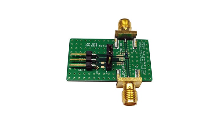
BGS8L2 LTE LNA with bypass switch evaluation board.
The BGS8L2 LTE LNA evaluation board simplifies the evaluation of the BGS8L2 LNA for the LTE application. The evaluation board enables testing of the device performance and requires no additional support circuitry. The board is fully assembled with the BGS8L2, the input series inductor and a decoupling capacitor. The board is supplied with two SMA connectors for input and output connection to RF test equipment. The BGS8L2 can operate from a 1.5 V to 3.1 V single supply and consumes about 5.2 mA.

BGS8L2 LTE LNA with bypass switch evaluation board.
| Distributor | Region | Inventory | Inventory Date | Order |
|---|
Upon selection of a preferred distributor, you will be directed to their web site to place and service your order. Please be aware that distributors are independent businesses and set their own prices, terms and conditions of sale. NXP makes no representations or warranties, express or implied, about distributors, or the prices, terms and conditions of sale agreed upon by you and any distributor.
1 design file
Please wait while your secure files are loading.