Getting Started with the EVBMA7318AIO Evaluation Board
Contents of this document
-
Out of the Box
-
Get Hardware
Sign in to save your progress. Don't have an account? Create one.

Purchase your EVBMA7318AIO
1. Out of the Box
The NXP analog product development board provides an easy-to-use platform to evaluate NXP products. The board supports a range of analog, mixed-signal and power solutions. They incorporate monolithic integrated circuits (ICs) and system-in-package (SiP) based on proven high-volume technologies. NXP products offer longer battery life, smaller form factors, reduced component counts, lower system cost and improved performance for powering state-of-the-art systems. This page will guide you through the process of setting up and using the EVBMA7318AIO evaluation board (EVB).
1.1 Kit Contents
The EVBMA7318AIO kit's contents include:
- EVBMA7318AIO reference design board
- Two battery simulation cables with cell simulation boards for battery cell controller (BCC) power supply and cell simulation through series resistors
- One transformer physical layer (TPL) daisy-chain cable for communication with other boards
- One current measurement cable to connect a shunt for current measurement
- One low-voltage cable to supply the system basis chip (SBC) and support controller area network (CAN) communication
- One high-voltage point measurement cable to support three high-voltage point measurements
- One USB Type-C-to-USB cable x1-cable to communicate with controller PC
1.2 Additional Hardware
No additional hardware is required for device evaluation. In addition to the kit contents, the following hardware is beneficial when working with this kit:
- 12 V direct current (VDC) power supply with 500 mA current capability
- 24 VDC power supply with 500 mA current capability or a 4-to-18-cell battery pack
- USB Multilink FX debug probe
- External shunt and current resource that can be connected to SHUNT (optional)
- Battery emulator board BATT-7318EMU (optional)
- 5 VDC power supply with 500 mA current capability (optional)
1.3 Minimum System Requirements
You will need a Windows PC workstation to evaluate the board.
For best results, please use the following operating systems:
- Windows® 11/10/8/7, Windows XP or Vista in 32-bit or 64-bit version
2. Get Hardware
This section covers the EVB components and features.
2.1 Board Features
The EVBMA7318AIO EVB includes the following features:
- Flexible battery management system (BMS) architecture
- Two BMA7318 on one board
- Cell voltage measurement for up to 18 battery cells per BMA7318 device
- 10 or 12 temperature-sensing channels per BMA7318 device
- Isolated serial peripheral interface (SPI) communication between the first BMA7318 device and the MCU without a TPL transceiver
- Off-board TPL communication with transformer isolation
- Cell balancing current up to 300 mA
- Low-cost SBC (FS23) and MCU (S32K312) implemented
- One CAN interface for communication with an upper controller or GUI
- One external universal asynchronous receiver-transmitter (UART) interface for communicating with the GUI
- Joint Test Action Group (JTAG) debugging interface
- High electromagnetic compatibility (EMC) performance
2.2 Board Description
The EVBMA7318AIO evaluation board includes two BMA7318 devices controlled by one MCU. Each BMA7318 device measures lithium-ion battery parameters for four to 18 cells. The first BMA7318 communicates with the MCU through isolated SPI and communicates with the second BMA7318 by TPL and transformer isolation. The off-board TPL uses transformer isolation. The MCU is supplied by an SBC that is powered by the 12 VDC power source. Figure 1 below illustrates the board's orientation.

2.3 Board Components
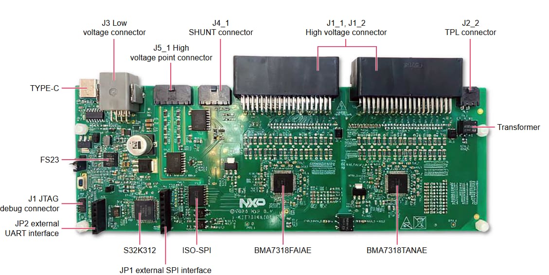
As shown below, Figure 2 identifies important components on the board. Table 1 (followed by additional tables) provides additional details on these components.
| Number | Devices | Description |
|---|---|---|
| 1 | BMA7318FAIAE | 18-channel lithium-ion battery cell controller (BCC) integrated circuit (IC) with serial peripheral interface-to-transformer physical layer (SPI-to-TPL) communication bridge and current measurement channel |
| 2 | BMA7318TANAE | 18-channel lithium-ion BCC IC with TPL communication and no current measurement channel |
| 3 | FS23 | SBC with CAN physical layer (PHY) and internal power supply for MCU |
| 4 | S32K312 | 32-bit MCU |
2.4 Connectors
| Pin | Name | Description |
|---|---|---|
| 1 | VCC | Power supply for JTAG debugging tool |
| 2 | JTAG_TMS | JTAG test mode selection |
| 3 | GND | Ground |
| 4 | JTAG_TCLK | JTAG test clock |
| 5 | GND | Ground |
| 6 | JTAG_TDO | JTAG data out |
| 7 | NC | Not connected |
| 8 | JTAG_TDI | JTAG data in |
| 9 | GNDDetect | GND detection |
| 10 | JTAG_RSTB | JTAG reset |
| Pin | Name | Description |
|---|---|---|
| 1 | NC | Not connected |
| 2 | NC | Not connected |
| 3 | NTC6 | Connect to an external negative temperature coefficient (NTC) thermistor for temperature sensing |
| 4 | NTC5 | Connect to an external NTC thermistor for temperature sensing |
| 5 | NC | Not connected |
| 6 | NC | Not connected |
| 7 | NC | Not connected |
| 8 | NC | Not connected |
| 9 | GND | Ground of BCC |
| 10 | C1P | Cell 1 voltage sensing point |
| 11 | C3P | Cell 3 voltage sensing point |
| 12 | C5P | Cell 5 voltage sensing point |
| 13 | C6Pb | Cell 6 voltage sensing point b |
| 14 | C8P | Cell 8 voltage sensing point |
| 15 | C10P | Cell 10 voltage sensing point |
| 16 | C12Pa | Cell 12 voltage sensing point b |
| 17 | C13P | Cell 13 voltage sensing point |
| 18 | C15P | Cell 15 voltage sensing point |
| 19 | C17P | Cell 17 voltage sensing point |
| 20 | VPWR | Power supply for the BCC |
| 21 | NC | Not connected |
| 22 | NC | Not connected |
| 23 | NC | Not connected |
| 24 | GND | Ground of NTC thermistors |
| 25 | GND | Ground of NTC thermistors |
| 26 | GND | Ground of NTC thermistors |
| 27 | GND | Ground of NTC thermistors |
| 28 | GND | Ground of NTC thermistors |
| 29 | GND | Ground of NTC thermistors |
| 30 | C0M | Cell 0 voltage sensing point |
| 31 | C2P | Cell 2 voltage sensing point |
| 32 | C4P | Cell 4 voltage sensing point |
| 33 | C6Pa | Cell 6 voltage sensing point a |
| 34 | C7P | Cell 7 voltage sensing point |
| 35 | C9P | Cell 9 voltage sensing point |
| 36 | C11P | Cell 11 voltage sensing point |
| 37 | C12Pb | Cell 12 voltage sensing point b |
| 38 | C14P | Cell 14 voltage sensing point |
| 39 | C16P | Cell 16 voltage sensing point |
| 40 | C18P | Cell 18 voltage sensing point |
| Pin | Name | Description |
|---|---|---|
| 1 | AIN10 | Should connect to an external NTC thermistor for temperature sensing |
| 2 | NTC7 | Connect to external NTC thermistors for temperature sensing |
| 3 | NTC6 | Connect to external NTC thermistors for temperature sensing |
| 4 | NTC5 |
Connect to external NTC thermistors for temperature sensing |
| 5 | NTC4 |
Connect to external NTC thermistors for temperature sensing |
| 6 | NTC3 |
Connect to external NTC thermistors for temperature sensing |
| 7 | NTC2 |
Connect to external NTC thermistors for temperature sensing |
| 8 | NTC1 |
Connect to external NTC thermistors for temperature sensing |
| 9 | GND | Ground for BCC |
| 10 | C1P | Cell 1 voltage sensing point |
| 11 | C3P | Cell 3 voltage sensing point |
| 12 | C5P | Cell 5 voltage sensing point |
| 13 | C6Pb | Cell 6 voltage sensing point b |
| 14 | C8P | Cell 8 voltage sensing point |
| 15 | C10P | Cell 10 voltage sensing point |
| 16 | C12Pa | Cell 12 voltage sensing point b |
| 17 | C13P | Cell 13 voltage sensing point |
| 18 | C15P | Cell 15 voltage sensing point |
| 19 | C17P | Cell 17 voltage sensing point |
| 20 | VPWR | Power supply for the BCC |
| 21 | AIN11 | Should connect to an external NTC thermistor for temperature sensing |
| 22 | NTC8 | Connect to external NTC thermistors for temperature sensing |
| 23 | NTC9 | Connect to external NTC thermistors for temperature sensing |
| 24 | GND |
Ground for NTC thermistors |
| 25 | GND |
Ground for NTC thermistors |
| 26 | GND |
Ground for NTC thermistors |
| 27 | GND |
Ground for NTC thermistors |
| 28 | GND |
Ground for NTC thermistors |
| 29 | GND |
Ground for NTC thermistors |
| 30 | C0M | Cell 0 voltage sensing point |
| 31 | C2P | Cell 2 voltage sensing point |
| 32 | C4P | Cell 4 voltage sensing point |
| 33 | C6Pa | Cell 6 voltage sensing point a |
| 34 | C7P | Cell 7 voltage sensing point |
| 35 | C9P | Cell 9 voltage sensing point |
| 36 | C11P | Cell 11 voltage sensing point |
| 37 | C12Pb | Cell 12 voltage sensing point b |
| 38 | C14P | Cell 14 voltage sensing point |
| 39 | C16P | Cell 16 voltage sensing point |
| 40 | C18P | Cell 18 voltage sensing point |
| Pin | Name | Description |
|---|---|---|
| 1 | B2-H_INOUT+ | Positive of TPL_H twisted wire on BMA7318TANAE |
| 2 | B2-H_INOUT- | Negative of TPL_H twisted wire on BMA7318TANAE |
| Pin | Name | Description |
|---|---|---|
| 1 | FS23_CANL | CAN bus negative (low) |
| 2 | FS23_CANH | CAN bus positive (high) |
| 3 | VBAT | 12 VDC power supply for the MCU |
| 4 | VBAT | 12 VDC power supply for the MCU |
| 5 | NC | Not connected |
| 6 | NC | Not connected |
| 7 | KL15_WKP | Wake-up source from KL15 |
| 8 | GND | MCU ground |
| Pin | Name | Description |
|---|---|---|
| 1 | B1-GND | Ground of BMA7318FAIAE |
| 2 | B1-ISENSE- | Current measurement wire is negative |
| 3 | B1-ISENSE+ | Current measurement wire is positive |
| 4 | B1-NTC-SHUNT | Temperature monitoring NTC for shunt |
| Pin | Name | Description |
|---|---|---|
| 1 | PACK+ | PACK+ high-voltage measurement point |
| 2 | NC | Not connected |
| 3 | LINK+ | LINK+ high-voltage measurement point |
| 4 | NC | Not connected |
| 5 | LINK- | LINK- high-voltage measurement point |
| Pin | Name | Description |
|---|---|---|
| 1 | VDD_MCU | Power supply from MCU |
| 2 | GND | MCU ground |
| 3 | EXT_CSB | SPI chip select input from an external device |
| 4 | EXT_SCLK | SPI clock input from an external device |
| 5 | EXT_MOSI | SPI controller output, target input from an external device |
| 6 | EXT_MISO | SPI controller input, target output to an external device |
| 7 | NC | Not connected |
| 8 | NC | Not connected |
| Pin | Name | Description |
|---|---|---|
| 1 | NC | Not connected |
| 2 | NC | Not connected |
| 3 | UART_RX_S32K | UART receive wire (signal) for the S32K312 |
| 4 | UART_TX_S32K | UART transmit wire (signal) for the S32K312 |
| 5 | GND | GND: MCU ground |
| 6 | VDD_MCU | Power supply from MCU |
Design Resources
Board Information
Additional References
- EVBMA7318AIO: Detailed information on this board, including documentation, downloads, software and tools
- BMA7318: Detailed information on BMA7318, 18-Channel lithium-ion battery cell controller IC
- S32K312: 32-bit Automotive General-Purpose Microcontroller
- FS23: Safety SBC Family with Power Management, CAN and LIN