Getting Started with the PF9453UK-EVK
Contents of this document
-
Out of the Box
-
Get to Know the Hardware
-
Configure Hardware
Sign in to save your progress. Don't have an account? Create one.
Purchase your PF9453 WLCSP Evaluation Board
1. Out of the Box
The NXP analog product development boards provide an easy-to-use platform for evaluating NXP products. The boards support a range of analog, mixed-signal and power solutions. They incorporate monolithic integrated circuits and system-in-package devices that use proven high-volume technology. NXP products offer longer battery life, a smaller form factor, reduced component counts, lower cost, and improved performance in powering state-of-the-art systems.
This page will guide you through the process of setting up and using the PF9453UK-EVK board.
1.1 Kit Contents and Packing List
The kit contents include:
- Assembled and tested evaluation board in an antistatic bag
- Quick Start Guide
- One PF9453UK-EVK evaluation board for evaluating board functions and features
- One USB type C cable
1.2 Additional Hardware
In addition to the kit components, the following hardware is recommended when working with this kit:
- Power supply with a range of 2.7 V to 5.0 V (set the current limit initially to 1.0 A; maximum power consumption at default voltages is up to 18 W)
- Oscilloscope/multimeter
- Electronic load (optional) - each power rail output can be connected to e-load for testing
1.3 Minimum System Requirements
This evaluation board requires a Windows PC workstation. Meeting these minimum specifications supports proper operation of this evaluation board:
- USB-enabled computer with Windows 7, Windows 8, or Windows 10
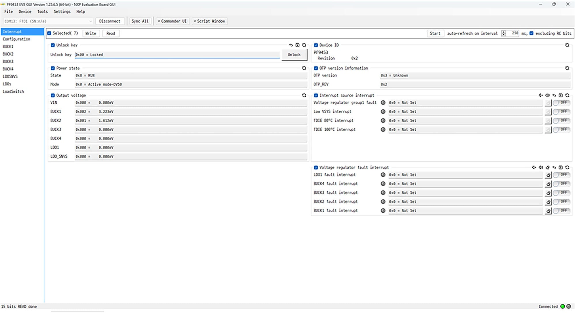
1.4 Software
Installing software is necessary to work with this evaluation board. All listed software is available on the evaluation board's information page at PF9453UK-EVK board or from the provided link.
- Go to PF9453 EVB graphical user interface
- Extract the Evaluation Kit GUI zip file,
PF9453_EVB_GUI_1.25.2.21-x64, into the selected folder. No need to install. (If the password is requested to unzip, type “NXP”) - Install the FTDI D2XX direct drivers from ftdchip
- Run the file
PF9453.exe. The interface window is shown in Figure 1
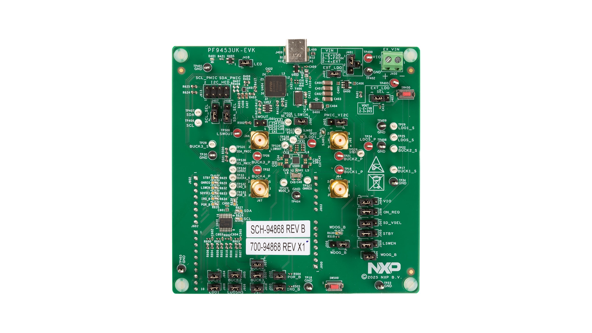
2. Get to Know the Hardware
This evaluation board features the PF9453 PMIC. The kit integrates all hardware needed to fully evaluate the PMIC and a communication bridge based on Future Technology Devices International Ltd. (FTDI) to interface with the PF9453 GUI software interface to configure and control the PMIC.
2.1 Board Features
- Four Buck regulators:
- One 2.5 A BUCK regulator
- One 1.5 A BUCK regulator with DVS
- Two 1 A BUCK regulators
- Two Linear regulators:
- One 10 mA LDO
- One 250 mA LDO
- One 400 mA load switch with a built-in active discharge resistor
- 32.768 kHz Crystal oscillator driver and buffer output
- System features:
- 2.7 V to 5.5 V operating input voltage range
- Power ON/OFF control
- Standby/run mode control
- DVS control
- Interrupt configuration
- Fm+ 1 MHz I²C Interface (via FTDI USB to I²C cable)
2.2 Board Description
The figure helps to identify the different main sections on the board.
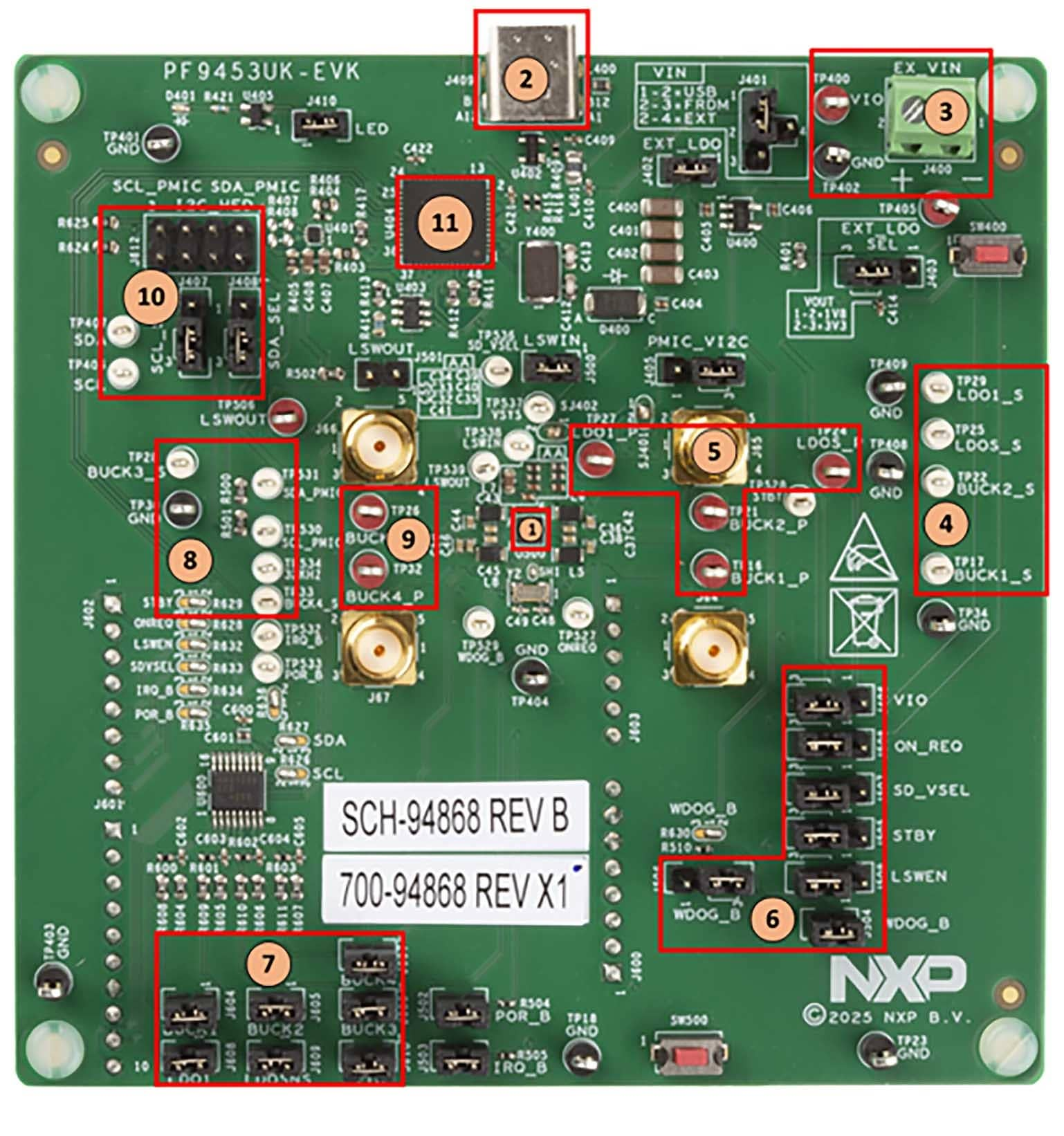
- PF9453 PMIC (WLCSP package)
- USB type C connector
- VPWR and GND input power connectors
LDO1,LDO_SNVS,BUCK1andBUCK2sensing test pointsLDO1,LDO_SNVS,BUCK1andBUCK2power test points- Digital signals jumper selectors
- ADC Jumpers
BUCK3andBUCK4sensing test points, SDA and SCL PMIC, 32 kHzBUCK3andBUCK4power test points- I²C headers and tests points
- FTDI (I²C to USB IC)
3. Configure Hardware
3.1 Configure Hardware
Figure 3 shows the default jumper configuration of the board.
| Name | Default | Description |
|---|---|---|
J401 |
1 to 2 | Selects source voltage for VSYS and PSYS (PMIC input voltage): 1 to 2 → PMIC input voltage comes from the USB type C connector 2 to 4 → PMIC input voltage comes from external connector (J400) or test points TP400 and TP402 2 to 3 → PMIC input voltage comes from FRDM_VIN Connector J600-06. |
J402 |
CLOSED | Connects the external LDO to VIN voltage. |
J403 |
1 to 3 | Selects output voltage of the external LDO U400: 1 to 2 → External LDO output voltage = 1.8 V 2 to 3 → External LDO output voltage = 3.3 V. |
J405 |
2 to 3 | Selects PMIC I²C pullup voltage: 1 to 2 → I²C Voltage comes from BUCK4 Out 2 to 3 → I²C Voltage comes from External LDO U400. |
J406 |
2 to 3 | Selects PMIC pullup voltage for digital signals: 1 to 2 → VIO Voltage comes from LDO_SNVS 2 to 3 → VIO Voltage comes from External LDO U400. |
J407 |
2 to 3 | Selects if SCL_PMIC signal (PMIC I²C signal) passes through the level shifter U401 or not: 1 to 2 → SCL_PMIC signal passes through level shifter U401 2 to 3 → SCL_PMIC signal does not pass through level shifter U401. |
J408 |
2 to 3 | Selects if SDA_PMIC signal (PMIC I²C signal) passes through the level shifter U401 or not: 1 to 2 → SDA_PMIC signal passes through level shifter U401 2 to 3 → SDA_PMIC signal does not pass through level shifter U401. |
J410 |
Closed | Connects the green LED driver U405 to VIN voltage. |
J500 |
Closed | Connects load switch Input to BUCK4 out. |
J501 |
Open | Jumper for internal validation only. |
J502 |
Closed | Connects POR_B signal to VIO pullup voltage. |
J503 |
Closed | Connects IRQ_B signal to VIO pullup voltage. |
J504 |
Closed | Connects WDOG_B signal to SW500. |
J505 |
2 to 3 | Selects PMIC_STBY_REQ signal voltage level: 1 to 2 → PMIC_STBY_REQ connected to VIO 2 to 3 → PMIC_STBY_REQ connected to GND. |
J506 |
2 to 3 | Selects WDOG_B signal voltage level: 1 to 2 → WDOG_B connected to VIO 2 to 3 → WDOG_B connected to GND. |
J507 |
2 to 3 | Selects SD_VSEL signal voltage level: 1 to 2 → SD_VSEL connected to VIO 2 to 3 → SD_VSEL connected to GND. |
J508 |
2 to 3 | Selects PMIC_ON_REQ signal voltage level: 1 to 2 → PMIC_ON_REQ connected to VIO 2 to 3 → PMIC_ON_REQ connected to GND. |
J509 |
2 to 3 | Selects LSW_EN signal voltage level: 1 to 2 → LSW_EN connected to VIO 2 to 3 → LSW_EN connected to GND. |
J604 |
Closed | Connects BUCK1_OUT voltage to ADC0 channel. |
J605 |
Closed | Connects BUCK2_OUT voltage to ADC1 channel. |
J606 |
Closed | Connects BUCK3_OUT voltage to ADC2 channel. |
J607 |
Closed | Connects BUCK4_OUT voltage to ADC3 channel. |
J608 |
Closed | Connects LDO1_OUT voltage to ADC4 channel. |
J609 |
Closed | Connects LDO_SNVS voltage to ADC5 channel. |
J610 |
Closed | Connects VIN voltage to ADC6 channel. |
| Name | Signal | Description |
|---|---|---|
| SJ401 | CLOSED | Connects VIN to PSYS. |
| SJ402 | CLOSED | Connects VIN to VSYS. |
| R626 | 1 to 2 | Selects SCL signal source: 1 to 2 → SCL signal comes from FTDI IC 2 to 3 → SCL signal comes from FRDM connector J601-10. |
| R627 | 1 to 2 | Selects SDA signal source: 1 to 2 → SDA signal comes from FTDI IC 2 to 3 → SDA signal comes from FRDM connector J601-09. |
| R628 | 1 to 3 | Selects PMIC_ON_REQ signal source: 1 to 2 → PMIC_ON_REQ signal comes from FTDI IC 1 to 3 → PMIC_ON_REQ signal comes from FRDM connector J602-01. |
| R629 | 1 to 3 | Selects PMIC_STBY_REQ signal source: 1 to 2 → PMIC_STBY_REQ signal comes from FTDI IC 1 to 3 → PMIC_STBY_REQ signal comes from FRDM connector J602-02. |
| R630 | 1 to 3 | Selects WDOG_B signal source: 1 to 2 → WDOG_B signal comes from FTDI IC 1 to 3 → WDOG_B signal comes from FRDM connector J602-03. |
| R632 | 1 to 3 | Selects LSW_EN signal source: 1 to 2 → LSW_EN signal comes from FTDI IC 1 to 3 → LSW_EN signal comes from FRDM connector J602-05. |
| R633 | 1 to 3 | Selects SD_VSEL signal source: 1 to 2 → SD_VSEL signal comes from FTDI IC 1 to 3 → SD_VSEL signal comes from FRDM connector J606-06. |
| R634 | 1 to 3 | Selects IRQ_B signal source: 1 to 2 → IRQ_B signal comes from FTDI IC 1 to 3 → IRQ_B signal comes from FRDM connector J606-07. |
| R635 | 1 to 3 | Selects POR_B signal source: 1 to 2 → POR_B signal comes from FTDI IC 1 to 3 → POR_B signal comes from FRDM connector J606-08. |
| R636 | 1 to 3 | Selects ADC supply voltage source: 1 to 2 → ADC voltage comes from FTDI_3.3V 1 to 3 → ADC voltage comes from FRDM_3.3V connector J600-05. |
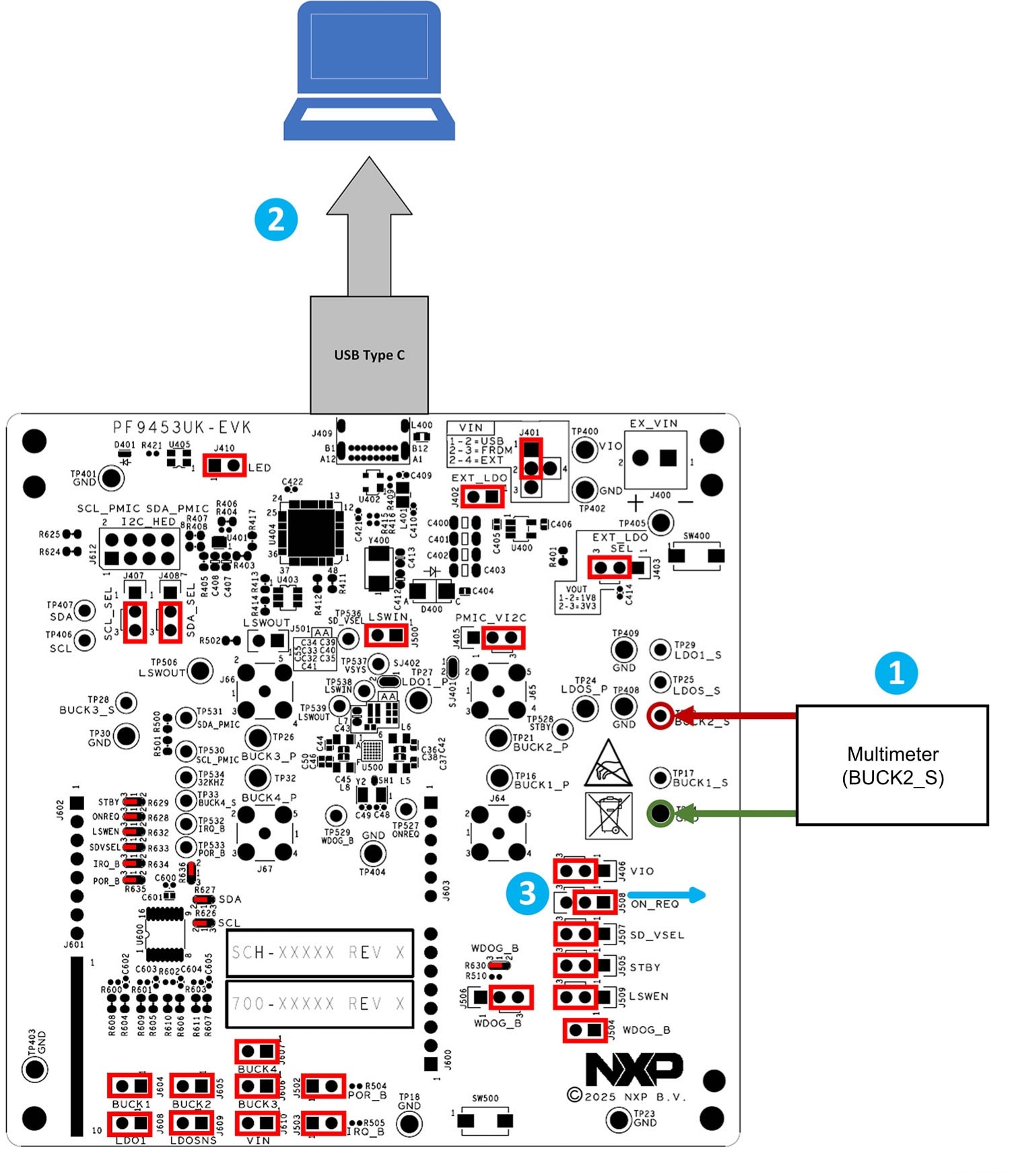
See Figure 4 and follow the steps to test the PF9453UK-EVK board. Ensure that all jumpers are in their default positions before starting (see Figure 3).
- Connect the positive terminal of the multimeter to
TP22BUCK2_Stest point and the negative terminal of the multimeter toTP34GND test point, see Figure 4 where step 1 is represented with the circle with number 1 - Connect the USB -Type C to the PF9453 WLCSP-EVK. See that the green LED
D401is ON, see Figure 4 circle with number 2. Use the USB Type-C connector as the power supply with this configuration. Avoid connecting loads that may exceed its power capacity. For tests requiring higher current—such as efficiency measurements—use an external power supply. See Table 3 for setup instructions. If the USB Type-C supply is sufficient, proceed to the next step - Move the
J508to positionJ508(1 to 2), see Figure 4, circle with number 3 (this turns on the PMIC by setting the high state thePMIC_ON_REQpin) - Measure the default voltage of
BUCK2with the multimeter, it must be 0.85 V (default voltage) - The default power configuration can be checked without doing any hardware (HW) or software (SW) modifications. Check the default voltage configuration using a multimeter on
BUCK1,BUCK2,BUCK3,BUCK4,LDO1and LDO SNVS test points
| Regulator | PF9453 |
|---|---|
BUCK1 |
1.1 V |
BUCK2 |
0.85 V |
BUCK3 |
1.8 V |
BUCK4 |
3.3 V |
| LDO1 | 0.8 V |
| LDO SNVS | 1.8 V |
Design Resources
Board Documents
Additional References
In addition to our PF9453 Product description page, you may also want to visit: