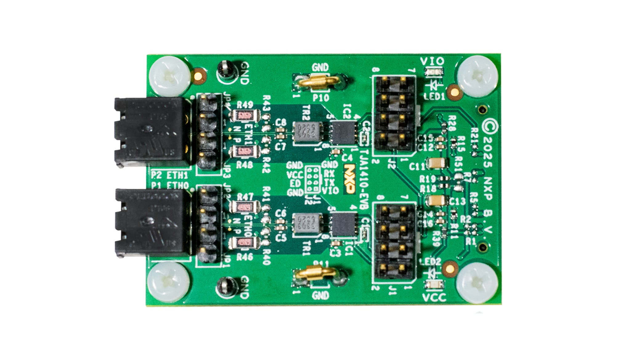
2. Get to Know the Hardware
2.1 Board Features
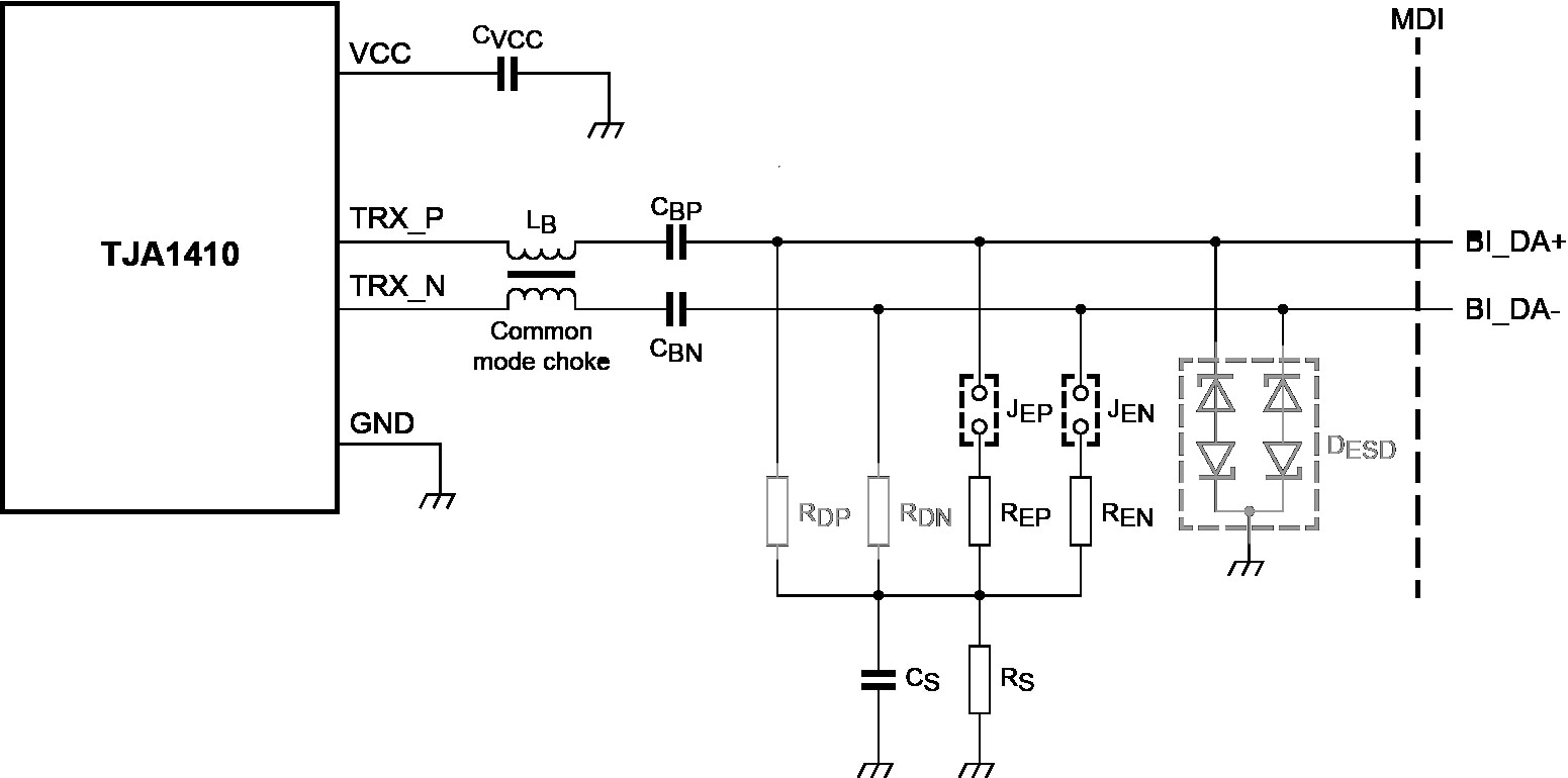
The TJA1410-EVB incorporates two 10BASE-T1S PMD transceiver channels, which consist of:
- TJA1410A 10BASE-T1S Ethernet physical medium dependent (PMD) transceiver
- End-node termination jumper
- Medium-dependent interface (MDI) connector
- Two OPEN Alliance PMD transceiver interface connector options
- Supply indicator LEDs
- Two 240 μH common mode chokes (CMC)
2.3 Evaluation Board Featured Components
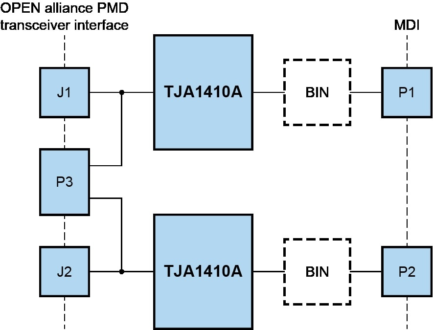
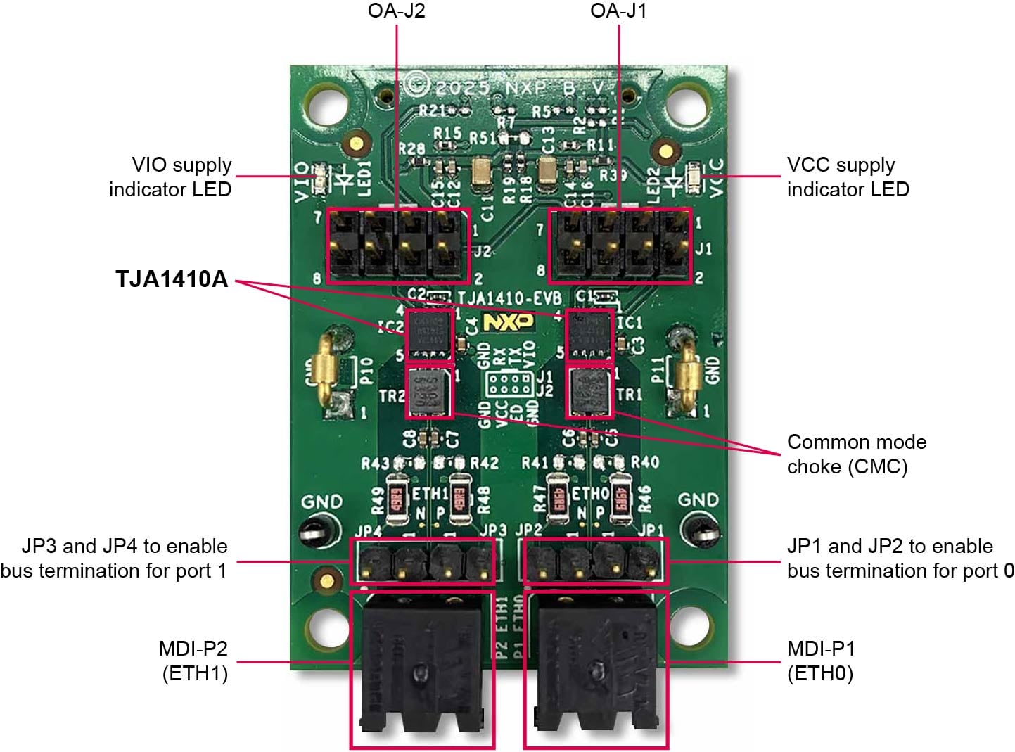
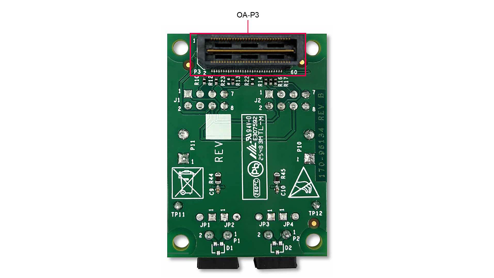
Figure 2 provides an overview of the TJA1410-EVB and shows the location of components on the board. On the bottom side of the TJA1410-EVB, shown in Figure 3, a connector (OA-P3) can be used instead of OA-J1 and OA-J2. Table 1 provides additional details about these components.
Table 1. Evaluation board components
| Number |
Description |
| OA-J1 |
Digital interface and supply connector for OPEN Alliance 10BASE-T1S PMD transceiver of port 1 |
| OA-J2 |
Digital interface and supply connector for OPEN Alliance 10BASE-T1S PMD transceiver of port 2 |
| OA-P3 |
Digital interface and supply connector for OPEN Alliance 10BASE-T1S PMD transceiver of port 1 and 2 |
VIO supply indicator LED |
VIO supply indicator LED is on when VIO supply is available |
| VCC supply indicator LED |
VCC supply indicator LED is on when VCC supply is available |
| TJA1410A |
OPEN Alliance 10BASE-T1S PMD transceiver variant for 3.3 V VIO supply |
| Common mode choke (CMC) |
CMC compliant to OPEN Alliance 10BASE-T1S EMC test specification for common mode chokes |
JP1 and JP2 bus termination for port 0 |
Jumper pins provide bus termination for end nodes; both JP1 and JP2 must be fitted with jumper sockets to enable end-node termination on port 0 |
JP3 and JP4 bus termination for port 1 |
Jumper pins provide bus termination for end nodes; both JP3 and JP4 must be fitted with jumper sockets to enable end-node termination on port 1 |
| MDI-P1 |
Medium-dependent interface for port 1 |
| MDI-P2 |
Medium-dependent interface for port 2 |
2.4 EVB Connectors
Table 2. OA-J1 and OA-J2
| Connector pin |
Signal |
Description |
| OA-Jx-1 |
VIO |
VIO interface supply voltage for TJA1410A; used to supply the digital I/O cells and the wake-up detection circuitry |
| OA-Jx-2, -7, -8 |
GND |
Ground |
| OA-Jx-3 |
TX_x |
TJA1410A transmits data signal |
| OA-Jx-4 |
ED_x |
TJA1410A energy detection signal |
| OA-Jx-5 |
RX_x |
TJA1410A receives data signal |
| OA-Jx-6 |
VCC |
Transceiver supply voltage for TJA1410A |
Table 3. OA-P3
| Connector pin |
Signal |
Description |
| OA-P3-28 |
VCC |
Transceiver supply voltage for TJA1410A |
| OA-P3-30 |
VIO |
VIO interface supply voltage for TJA1410A; used to supply the digital I/O cells and the wake-up detection circuitry |
| OA-P3-6, -44 |
GND |
Ground |
| OA-P3-4 |
TX_0 |
TJA1410A transmits data signal port 0 |
| OA-P3-8 |
RX_0 |
TJA1410A receives data signal port 0 |
| OA-P3-16 |
ED_0 |
TJA1410A energy detection signal port 0 |
| OA-P3-42 |
TX_1 |
TJA1410A transmits data signal port 1 |
| OA-P3-46 |
RX_1 |
TJA1410A energy detection signal port 1 |
| OA-P3-50 |
ED_1 |
TJA1410A receives data signal port 1 |
| OA-P3-1 |
(VCC) |
Alternative VCC pin assignment option via 0 Ω resistor configuration (default: not connected) |
| OA-P3-3 |
(VIO) |
Alternative VIO pin assignment option via 0 Ω resistor configuration (default: not connected) |
| OA-P3-11, -33 |
(GND) |
Alternative GNDpin assignment option via 0 Ω resistor configuration (default: not connected) |
| OA-P3-16 |
(TX_0) |
Alternative TX_0 pin assignment option via 0 Ω resistor configuration (default: not connected) |
| OA-P3-36 |
(RX_0) |
Alternative RX_0 pin assignment option via 0 Ω resistor configuration (default: not connected) |
| OA-P3-43 |
(ED_0) |
Alternative ED_0 pin assignment option via 0 Ω resistor configuration (default: not connected) |
Table 4. MDI-Px
| Connector pin |
Signal |
Description |
| MDI-Px-1 |
BI_DAx_n |
- Terminal of MDI connector |
| MDI-Px-2 |
BI_DAx_p |
+ Terminal of MDI connector |
2.5 EVB Jumpers
Table 5. Jumper configuration
| Jumper |
Config |
Description |
JP1 and JP2 |
OPEN |
Drop-node termination port 0 |
| CLOSED |
End-node termination port 0 |
JP3 and JP4 |
OPEN |
Drop-node termination port 1 |
| CLOSED |
End-node termination port 1 |
Table 6. LED status
| LED |
Status |
Description |
VIO LED |
ON |
VIO supply is on |
| OFF |
VIO supply is off |
VCC LED |
ON |
VCC supply is on |
| OFF |
VCC supply is off |