RoadLINK® SAF5400 Single Chip Modem for V2X
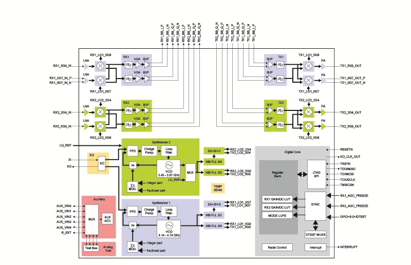
The TEF5100 transceiver architecture is based on direct conversion for both the transmitter and receiver, which eliminates expensive external filters. Internal, digitally controlled gain stages at RF and BB give the receiver both low noise figure and a large dynamic range.
The transmitter has several gain steps providing a wide output power range. The cut-off frequencies of the baseband filters are calibrated with an internal tuning loop and the filters support modulation bandwidths up to 20 MHz. The transceiver is controlled via a four-wire SPI interface. A high-speed parallel interface is provided to support fast gain control, RX/TX switching and frequency hopping. An internal auxiliary ADC is included for calibration purposes and to serve various external functions like power and temperature measurements. The TEF5100EL contains autonomous internal AGC functionality for the fast acquisition of packets.
To get further assistance directly from NXP, please see our Engineering Services.
1 engineering service

To find additional partner offerings that support this product, visit our Partner Marketplace.