Note: JN5189/88T is preferred for any new Zigbee®,
Thread design. No new software releases planned
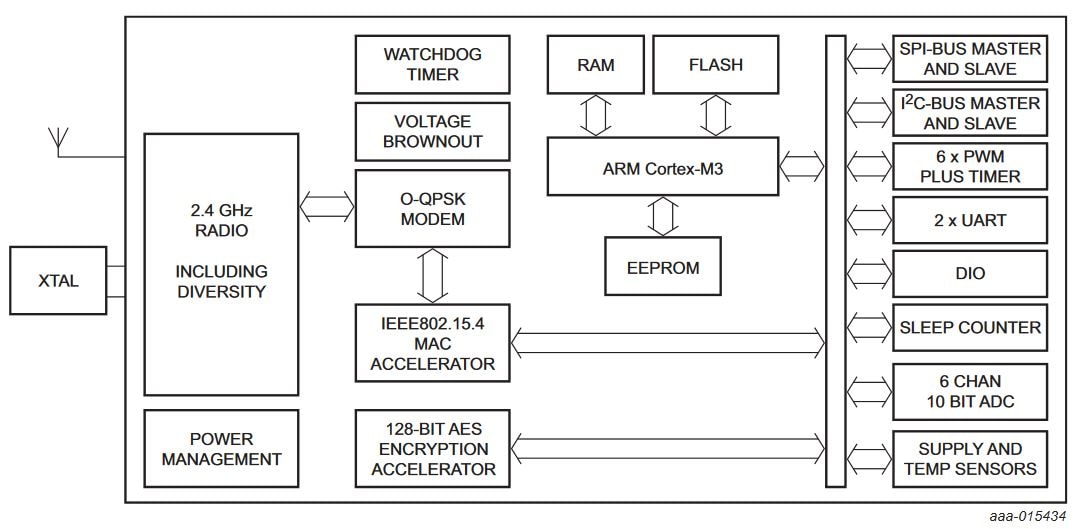
The JN5179 device is an ultra-low-power, high-performance wireless microcontroller, optimized as a platform for
ZigBee 3.0 applications in Smart Home and Smart Lighting networks. It features an Arm®
Cortex®-M3 processor with debug and programmable clock speeds. The JN5179 device has 512 kB of
embedded Flash memory as well as 32 kB of RAM and 4 kB of EEPROM. The embedded Flash can support
"Over-The-Air" firmware updates. The device also includes a 2.4 GHz "IEEE802.15.4 compliant"
transceiver and a comprehensive mix of on-chip analog and digital peripherals.
The radio transmit power is configurable up to +10 dBm output. The very-low receive operating current (down to 12.7
mA in normal operation and 0.6 µA in sleep mode) results in long battery life, allowing operation directly
from a coin cell. Through its power-saving modes, the device is therefore ideal for battery-powered nodes. The
on-chip peripherals include a fail-safe I²C-bus, SPI-bus ports (both leader and follower) and a 6-channel
analog-to-digital converter, directly supporting a wide range of applications without the need for extra hardware.
For support documentation, please click here.