As markets and industries continue to evolve, connectivity and security will
play a greater and greater role in their evolution. The term Internet of
Things (IoT) has been used quite extensively to express today’s world
of consumer and industrial products. However, for some time the
definition of IoT and more specifically, its application, has been confusing
to many. In its simplest terms it defines a network of products operating
independently yet connected in a way that allows interoperability with each
other.
Limiting the definition to these terms only describes the tip of the IoT
iceberg.
When designing for the IoT, products need certain key features
For a product to reside in the IoT ecosystem it needs to be as ready to go as
possible, with multiple features. Besides providing the product’s key
function, the devices and network need some or all of the following
attributes:
- Processing capability (MCU, Apps processor and/or MPU)
- Power management
- Memory
-
Connectivity (WiFi, Bluetooth, NFC, Bluetooth Low Energy, 15.4 Thread/ZigBee and/or Ethernet)
- Sensing
- A form of human or machine interface
- Software and firmware support including O/S and driver enablement
The end functionality of a specific IoT device will define the combination
and/or level of complexity of those integrated components. Clearly the
requirements for an end node product such as a wearable, medical monitoring
device will be very different from a high speed, high-bandwidth gateway
product.
Nothing stated above is a surprise to anyone, but what is emerging is how our
future IoT landscape is morphing and transforming. The process of developing
new products all the way up the supply chain remains fairly consistent
encompassing areas of process and materials R&D, IC design, hardware
development, the integration of software and firmware and then wrapping the
final product design and application development. The pace of product
introductions, especially those serving IoT markets, will continue to
accelerate. The level of integration and functionality will also continue to
increase exponentially. As a result, volumetric area and in some cases
weight, will become a clear hurdle to overcome.
There are simply too many startups. Too many $1B ‘wanna-be’
companies coming from incubators, split-off product teams and college
graduates with cool ideas. The standard NPI process simply won’t work.
Beyond their big ideas, these emerging companies have limited staffing,
usually limited funding and opportunity windows and very strong skills in a
few focused areas. What they need is a breath of experience in hardware system
design (Analog, Digital, RF, Sensors, high-speed memory, etc) as well as
software and firmware development, board and peripheral design, system design,
test and validation. All of this before they develop their unique
application and launch their cool product to market.
How our latest portfolio rises to the challenge
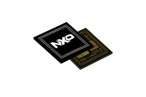
At NXP, we get it. We’re designing more integrated, optimized modules.
Designing smaller, packing more features and delivering simple, plug-and-play
solutions. There’s no better example than our Single Chip System (SCM)
families, which are making exciting things possible for IoT product designers.
Choose the right solution for you—three families comprise our SCM
portfolio
SCM-i.MX 6Dual/6Quad
This past February, NXP launched into production the first SCM family:
SCM-i.MX 6D/Q, which integrates in a very small module (14mm x 17mm) a NXP
high-end, fully featured i.MX6 Dual or Quad core application processor, a
fully enabled power management IC, embedded SPI NOR memory, plus over 100
discrete components which allow the module to perform as a truly integrated
system. In addition, you can choose either 1GB or 2GB of LPDDR2 memory.
Several derivatives are now being launched including meeting industrial
specification as well as the introduction of ePoP memory (512MB LPDDR2 + 4GB
eMMC combination) in place of the PoP LPDDR2 options.
Learn more about the SCM 6Dual | 6Quad
SCM-i.MX 6 SoloX
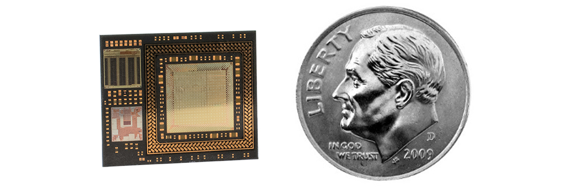
 One of our two newest families, the SCM-i.MX 6SX is a very small (13mm x
13mm) package combining the performance of NXP’s i.MX 6SoloX apps
processor, a PF100 power management device as well as over 40 discrete
components (decoupling caps, resistors). The part also comes with an option of
a varied size of LPDDR2 memory and ePoP, both in a Package on Package (PoP)
configuration. This product is designed in a 0.75mm diagonal ball pitch array
allowing you to design it in a relatively low-cost PCB board. The SCM-i.MX 6SX
also comes with a tested and validated BSP, allowing you to quickly design it
into your application and move quickly into developing your application
software and product.
These modules address time to market with most of the heavy lifting done by
NXP—from high speed memory design and calibration to optimizing the
power rails. In addition, these modules address size. In all cases, they offer
you a minimum 50% reduction in board area over discrete solutions. In most
cases, the area saved can be substantially higher.
Learn more at the SCM 6SoloX
SCM-i.MX 6 SoloX V-Link
SCM-i.MX 6SX V-Link P0.75mm is an exciting new product portfolio addressing
the next big challenge for those of you wanting to use a highly integrated
module while also getting your own unique, customizable solution specific for
your product and application. The first in this family is an integrated SCM
with a full featured i.MX 6SoloX apps processor, a full featured PF100 power
management IC as well as 512MB of LPDDR2 along with a host of discrete
components all embedded in a 15.5mm x 15.5mm base SCM package. In addition a
unique NXP signal bus (V-Link) has also been integrated inside of the package
allowing for multiple I/O signals, power and ground from the apps processor
and PMIC to be brought to the top surface along with several pass through
connection. This configuration now allows you to design, fabricate, assemble
and attach your own unique ‘top board’ using standard PCB or
substrate based technologies offered around the world. What is exciting about
this product is that NXP has developed a base SCM with the horsepower and
functionality required for that matched application, yet allowing you to pick
your own off-the-shelf components for the top board. These can be anything
from industry RF solutions (WiFi, NFC, classic BT, Bluetooth Low Energy, 15.4 or combination
modules) along with all types of sensor and charging devices to audio codex
including those offered by NXP or not. In addition, the V-Link has several
pass-through connections allowing direct access of the top board from your PCB
application board for components like specialty PHY interfaces. This allows
for additional space utilization yet still maintaining access from the main
board.
Learn more about SCM V-Link bus
So much more to come
These new SCM products, along with additional new families and derivatives,
are focused on:
- Ease of use
- High levels of integration
- Enhancing levels of software enablement and validation
- Time to market
-
System-level size reduction for both the consumer and industrial markets
As this class of products evolve, targeting the automotive markets will become
inevitable. With the introduction of the third family (SCM-i.MX 6 SoloX
V-Link), NXP brought to both established and new customers the next level of
customization they each require.
As exciting as these new products are,
you ain’t seen nothing yet.
The coming months and years will grow our level of sophistication and offer
you even more compelling options including higher levels of system security,
functionality, analytics, greater autonomy and ease of use. We’re
committed to making designing for the IoT an easier, simpler process with
ready-to-go solutions like the SCM families.
There’s more to come, so stay tuned.


 One of our two newest families, the SCM-i.MX 6SX is a very small (13mm x
13mm) package combining the performance of NXP’s i.MX 6SoloX apps
processor, a PF100 power management device as well as over 40 discrete
components (decoupling caps, resistors). The part also comes with an option of
a varied size of LPDDR2 memory and ePoP, both in a Package on Package (PoP)
configuration. This product is designed in a 0.75mm diagonal ball pitch array
allowing you to design it in a relatively low-cost PCB board. The SCM-i.MX 6SX
also comes with a tested and validated BSP, allowing you to quickly design it
into your application and move quickly into developing your application
software and product.


