In Figures 1 and 2 of my November 2015 post I
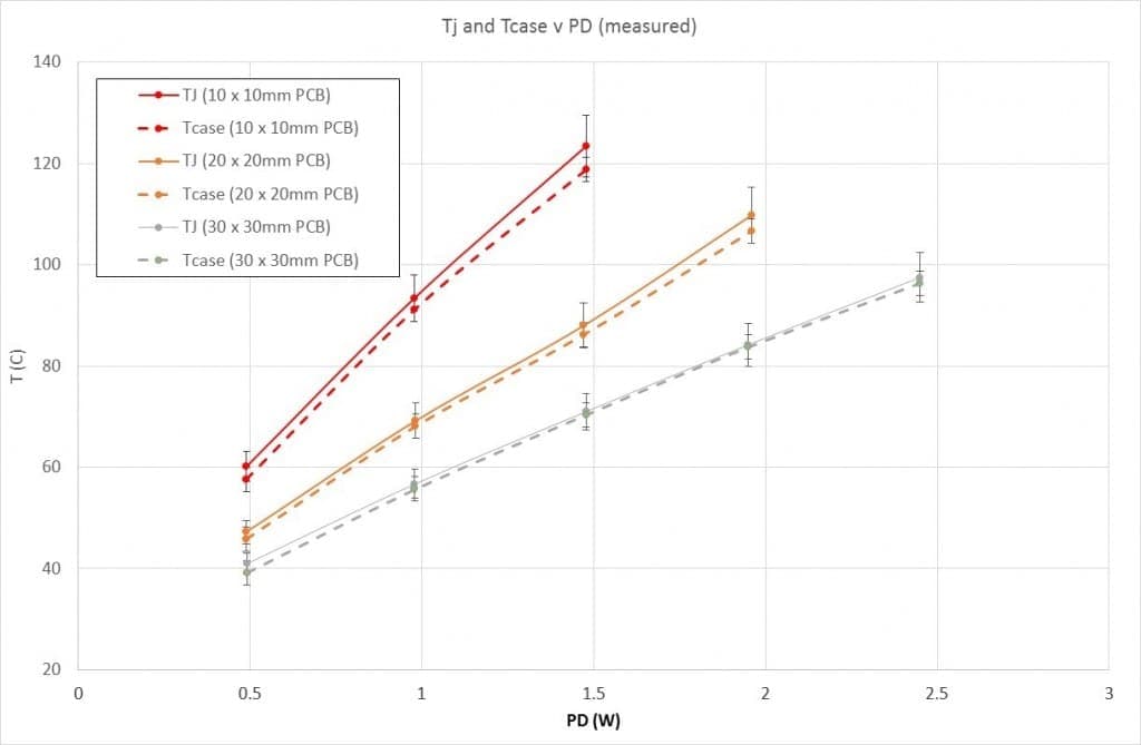
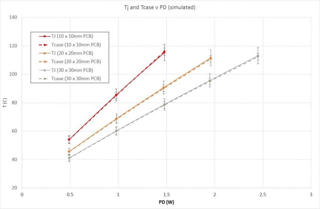
demonstrated how (for a fixed PD) the Tj of an LFPAK56 MOSFET under steady-state conditions
depends to a large extent on the area of PCB copper to which the device is soldered. This was shown in simulation
and verified by real-life experiment. The results from that earlier post are reproduced in Figure 1 below, for your
convenience.

Figure 1 Simulated Tj v PD for an LFPAK56 device on various
PCBs
In Figure 1, the vertical axis is device junction temperature Tj. However, for a fixed power dissipation
we could also redraw Figure 1 as a graph of junction-to-ambient thermal resistance
(“Rthj-a”) against PCB area. I’ve done this with the points highlighted in Figure 1,
and I’ve also added an extra board size of 1600mm2 so that we have a curve composed of four points
(Figure 2). Remember that

and Tamb in this case is 20°C.

Figure 2 Rthj-a v PCB copper area for an LFPAK56 device
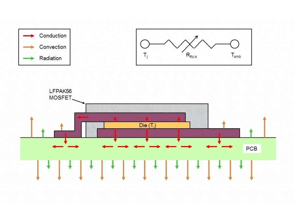
We can visualize Rthj-a as being the single lumped thermal resistance which represents the combination of
all the possible thermal pathways from the device die (junction) to ambient, as shown in Figure 3

Figure 3 Rthj-a represents the combination of all the possible thermal pathways from the device die to
ambient
As we saw in an earlier post, for a
surface-mount device using its own PCB as a heat sink, the majority of the die heat energy travels downwards into the
PCB and then to ambient from the surface of the PCB. This is what I have tried to show in Figure 3. I also have
shown the equivalent thermal resistance Rthj-a representing the aggregate of these paths.
Rthj-a is shown as a variable resistor because its value in any situation will depend on many factors
– not the least of which being PCB copper area, as we have just seen in Figure 2.
Let’s assume now that we’d like to add some more heatsinking to our MOSFET. Is there another way in
which we could assist the die thermal energy in its passage toward ambient? Would it help, for instance, if we put
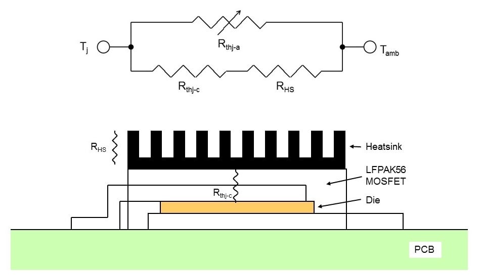
a heat sink on top of our device? If we know the thermal resistance through the top of the device
(Rthj-c), and the thermal resistance of the heat sink (RHS) could we combine these numbers with
the Rthj-a numbers in Figure 2 to give us an improved thermal network as shown in Figure 4?

Figure 4 Adding a heat sink to the top of the LFPAK56 device, and its new thermal
network.
Well it so happens that our helpful MOSFET supplier has given us a figure for Rthj-c of 34K/W, and the
manufacturer of a small finned 12 x 12mm heat sink is quoting an RHS figure of 25K/W. We also have the
Rthj-a figures for several sizes of PCB copper in Figure 2, so that’s everything we need,
isn’t it? Can we now estimate a new overall thermal resistance curve for the system of Figure 4 using simple
series/parallel combinations of resistors? And how would that compare to the original curve of Figure 2?
Interestingly, the answer turns out to be… Oh. Oh dear. I appear to have run out of space again. So, on that
cliffhanger I’ll leave you for this month. If you’d like to have a go at estimating the new thermal
resistance curve for the MOSFET plus heat sink, please feel free – I promise I have given you all the
information you need!


