A large part of thermal analysis work is concerned with carrying out ‘what if?’ analyses. For example, if I have a PCB with dissipating components on it I would probably like to know what temperatures those components will run at. But what if I add more components? What if I mount them closer together? What if I add a cooling fan? What difference does any of this make?
Similarly, as a MOSFET manufacturer, we might sometimes want to know the thermal consequences of varying a package design or changing the types of materials used in the package and so on.
Of course, it is possible to answer these questions by building and testing actual prototypes, and at some stage in the design process we will have to do this anyway. But in the early stages of a design or feasibility study it makes much more sense to carry out the investigations using simulation software, where changes to a configuration can be made easily and analysis of results viewed quickly. The thermal simulation package that we use for this purpose is Mentor Graphics’ FloTHERM® (other simulation packages are available), which allows thermal models to be built and simulated in a 3D CAD-style environment.
An obvious question at this point is: do we trust the simulations to give us reasonably accurate answers? I would say ‘yes’ for two reasons:
- the physics underpinning the simulations is well understood, and
- the people writing the software presumably know what they are doing.
So, assuming we use the software properly, we should be fairly confident of the results. Even so, from time to time it’s still good to carry out some calibration or ‘sanity check’ exercises, and it’s an example of one such exercise that I’d like to share in this post.
A real-life example
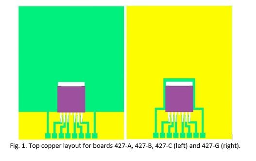
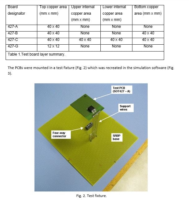
For this exercise, identical MOSFET devices were mounted on PCBs of the same overall size but with varying amounts of copper coverage. See Fig. 1 and Table 1.
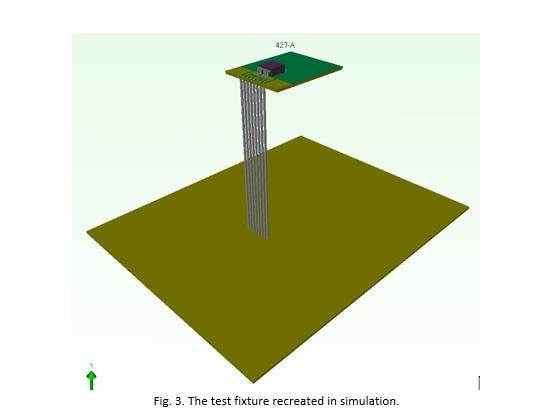
For each PCB configuration the MOSFET device was powered with a constant 1 W and allowed to reach a steady-state temperature. Each MOSFET had a calibrated on-die temperature sensor which allowed us to take extremely accurate measurements of junction temperature (TJ) in the steady state. The ambient temperature during each test was also recorded. The four PCBs were then recreated in simulation, with die dissipation set to 1 W and the steady-state temperatures recorded. The real and simulated results are recorded in Table 2, expressed as
thermal resistances
as described in the JESD51 series of
JEDEC standards.
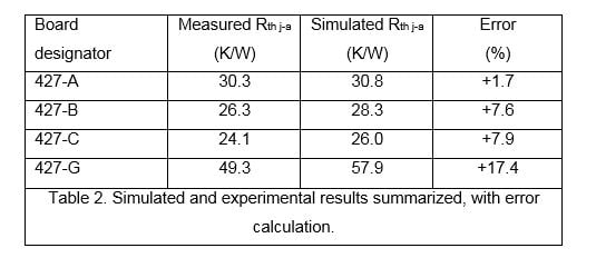
So how did we do?
Well, the A, B and C boards came very close to the measured result, but G still needs a little work. We must remember that not all the simulation input parameters can be known with absolute certainty – this being particularly true of material thermo-physical properties.
It is also worth remembering that our measurement of reality may not be perfect: all real-life test equipment has some degree of error associated with its measurements. There isn’t enough space in this post to explore these potential errors in detail, but it could certainly be the subject of a future blog post!
Next time: how simulation can help us look at what goes on in a device die at very short timescales.